
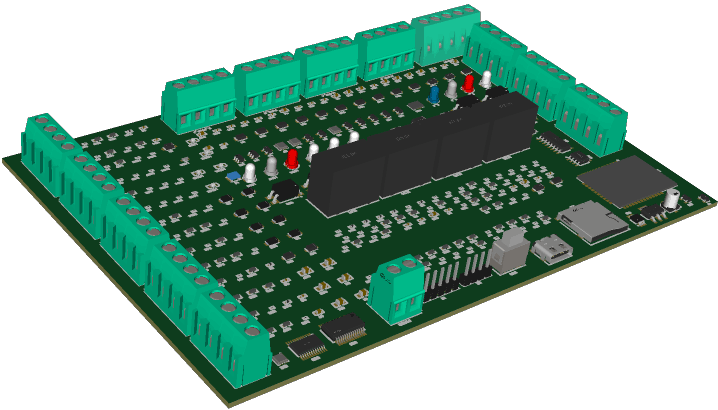
PCBs, or printed circuit boards, are the foundation of modern electronics. We discuss in this blog how to understand 8-layer PCBs with definitions, functions, applications, design information, and manufacturing processes associated with them.
What is an 8-layer PCB?
An 8-layer PCB is a multilayer PCB with eight layers of conductive material. These layers give the board a low profile and are sandwiched between dielectric materials, pressed, and heated to join poles together.
8-layer PCBs have the following advantages:
- Enhanced power distribution: Several power planes for steady functioning.
- Compact design: Greater utility in a more condensed space.
- Better signal integrity: reduced signal interference and managed impedance.
8-layer PCBs are best suited for applications where high reliability is required, such as RF transmission and high-speed digital systems.
Details of Layers in 8-Layer PCB Gerber
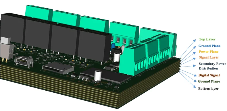
The comprehensive nature of such an eight-layer PCB is due to its structure comprising eight layers. Each of these layers is intended for different roles.
1. Top layer:
- Supports RF traces dedicated to Ka-band communication.
- Guarantees controlled impedance for applications with high-frequency requirements.
2. Layer 2 (ground plane):
- Acts as a cover against electromagnetic interference (EMI) to radio frequency traces.
- A stable reference plane ensures enhanced signal quality.
3. Layer 3 (power plane):
- Supplies three types of voltage (1.2, 3.3, and 5 volts).
- There is a reduction of noise using the correct decoupling and bypassing.
4. Layer 4 (signal layer):
- Handles communication buses such as SPI, I2C, and beam steering signals.
- Trace routing is performed so that interference between the traces is minimized.
5. Layer 5 (secondary power distribution):
- Provides power to circuits.
- Power lines are separated to avoid cross interference.
6. Layer 6 (digital signal layer):
- Supports fast signals for control systems, Wi-Fi, and USB.
- Short trace lengths with control are provided to ensure timing.
7. Layer 7 (ground plane):
- Separates power noise from digital signals.
- More shielding is provided for vulnerable transmissions.
8. Layer 8 (bottom layer):
- Provides a plane to distribute heat.
- Hold thermal vias that connect to a copper pour for enhanced heat management.
The arrangement of the layers is not fixed, and the above PCB layers are just for your reference. These neat and distinct layers of the 8-layer PCB ensure reliable operation even in harsh conditions.
Manufacturing of 8-layer PCB
There are a few procedures involved in the manufacturing of an 8-layer PCB:
- A Gerber file contains the copper layers, the drill data, the silkscreen, and the solder mask.
2. Material preparation:- Selection of proper materials such as PTFE or FR4.
- Certain requirements will decide the thickness of each layer.
3. Inner layer imaging and etching:- The inner layer's photoresist is used in printing exposed to UV light.
- Etching helps remove unneeded copper to form circuit-style layouts.
4. Lamination of layers:- The layers are stacked in alignment and precisely placed.
- To ensure the stack forms a solid structure, lamination is carried out with pressure and heat.
5. Drilling and plating:- Holes and vias are made to join the connecting layers.
- Copper is plated to provide positive electrical connections.
6. Outer layer imaging and etching:- The outer layers are patterned using a similar imaging and etching technique.
7. Application of solder mask:- A solder mask is applied to avoid short circuits and provide insulation.
8. Final finishing and testing:- Surface finishing like ENIG and HASL were done.
- To ensure performance requirements, electrical and quality tests are performed on the PCB.
This calls for sophisticated instruments and trained personnel for accuracy.
Advice on 8-Layer PCB Design
An 8-layer PCB may prove to be an uphill task in terms of the implementation processes. However, here is some advice on 8-layer PCB design:
1. Establish layers of clear responsibilities- Set a task for each layer, such as a cavity for receptors, a wide band, or a distribution of energy.
2. Signal integrity – central importance of the PCB design:- For high-speed traces, controlled impedance is recommended.
- To decrease interference, ground planes should be located next to signal layers.
3. Power distribution to be enhanced:- Where applicable, employ more than several power planes to ensure constant feeding.
- Use capacitors near the ICs to decouple power traces.
4. Evaluate thermal management strategies:- Patch thermal via to the bottom layer so that it can connect hot devices.
- Make use of copper pours to provide better heat dissipation.
5. Address the issue of crosstalk:- Maintain the symmetry and close differential pair paths.
- To minimize crosstalk, digital and analog signals should be routed on different planes.
6. Test the design:- Evaluate thermal effects and signal loss for instances by the use of simulation software.
- To help detect problems early on, perform DRCs.
7. Work with PCB manufacturers:- Ensure that your design is within the manufacturer's requirements, such as minimum via dimensions and trace widths.
If these tips and instructions are followed, you will be able to make 8-layer PCB boards that are reliable and efficient.
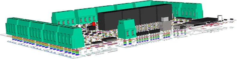
One-Stop 8-Layer PCB Manufacturer from R&D to Fabrication and Assembly
If you plan to develop an 8-layer PCB or PCBA project and need a turnkey PCB manufacturer with R&D capabilities to ensure the success of your project, you can work with the advanced PCB and PCBA manufacturer PCBONLINE.

Founded in 1999, PCBONLINE has two large advanced PCB manufacturing bases, one PCB assembly factory, stable supply chains, and an R&D team.
PCBONLINE has strong PCB fabrication capabilities, including FR4 PCBs from 1 to 64 layers, flexible PCBs up to 8 layers, rigid-flex PCBs from 2 to 24 layers, high-frequency PCBs from 4 to 24 layers, and copper-core PCBs from 1 to 8 layers.
Besides 8-layer PCB fabrication, PCBONLINE provides prototyping/sampling, component sourcing, PCB assembly, PCBA value-added, and box-build assembly until the finished device delivery.
PCBONLINE can provide software and hardware R&D or take part in your project's development from the early phase from the perspective of optimum PCB design.
Offers one-on-one engineering support and free design for manufacturing (DFM) and solves all technical issues to ensure smooth 8-layer PCB manufacturing and successful results of your project.
High-quality 8-layer PCB manufacturing certified with ISO 9001:2015, ISO 14001:2015, IATF 16949:2016, RoHS, REACH, UL, and IPC-A-600 Class 2/3.
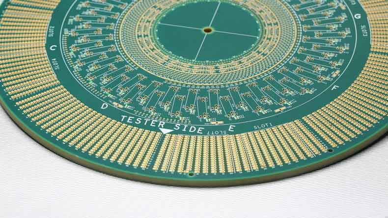
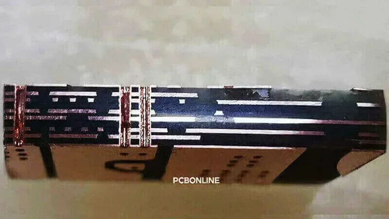
So far, PCBONLINE has manufactured many 8-layer PCBs in different materials for automotive, industrial, communications, computers, and consumer electronics. Below is an 8-layer copper-based PCB manufactured by PCBONLINE for vehicle front lights. To get a quote for an 8-layer PCB/PCBA project or PCBA in any other layer quantity, please contact info@pcbonline.com.
Conclusion
An 8-layer PCB is a robust solution for modern-day high-technology electronics. It has a multilayer structure which ensures great signal integrity, optimal power distribution, and efficient thermal mitigation. Understanding how each layer works and following best practices would help design great irrespective of the targeted system, be it high-speed digital systems or radio frequency systems. If you have questions about your 8-layer PCB, chat with PCBONLINE from the online chat window.
PCB fabrication at PCBONLINE.pdf


