Advantages of the PCB Assembler PCBONLINE
 MATERIALS
 At PCBONLINE, the component warehouse of the EMS PCBA factory has more than 10,000,000 types of passive and active components in stock, and we can source any components for PCB assembly quickly.
 EQUIPMENT
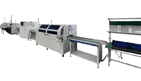
 The PCB assembly lines at PCBONLINE are completely equipped, including silkscreen printing, solder paste inspection, 3D X-ray, reflow soldering/nitrogen reflow, 3D AOI (automated optical inspection), wave soldering/selective soldering, etc.
 TEAM
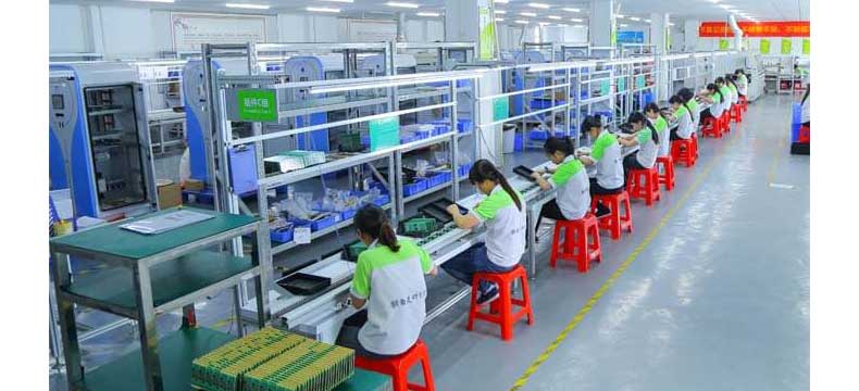
TEAM Own PCBA factory, in-house R&D team, 100+ engineers, and 500+ technicians to provide one-stop EMS PCBA solutions without minimum order requirements, including free DFT/DFM/DFA/DFX services.
 QUALITY
 Our PCB assembly includes BOM check, first article inspection, functional testing, etc, and is certified with ISO 9001:2015, 9001:2016, IATF 16949, REACH, RoHS, UL, and IPC-A-610 Class 2/3.
 CUSTOM
 The PCB assembler PCBONLINE provides custom PCBA manufacturing tailored to your demands. Besides printed circuit board assembly, we provide PCBA R&D, DFA, PCB fabrication, PCBA value-added, and box-build assembly.
 TRANSPORT
 Fast delivery, instant online quotation, reasonable price. The PCBA shipping methods include air, sea, and rail shipping by DHL, FedEx, and UPS.
Overview of the PCBA Process
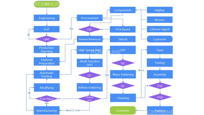
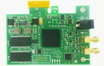
PCB assembly is mounting blank PCB boards with electronic components to make them into semi-finished devices. This process includes PCBA manufacturing and PCBA tests. In PCBONLINE, PCBA tests go through the whole process to ensure 100% product quality and customer satisfaction.
Roughly, the PCBA process can be divided into these phases: soldering paste printing > SMT (surface mounted technology) > reflow soldering > AOI (automated optical inspection)> THT (through-hole technology) > wave soldering > touch-up and cleaning > IC programming > FCT (functional tests) > aging testing.
In addition, for bulky PCBA manufacturing, we usually have an FAI (first article inspection) for the PCBA prototypes and send the FAI report for the client to review and approve before going to batch production.
PCBA Manufacturing
Step 1. BOM checking
Before assembly, our experienced engineers check your BOM (bill of materials). This makes sure that electronic components are okay for PCB assembly.
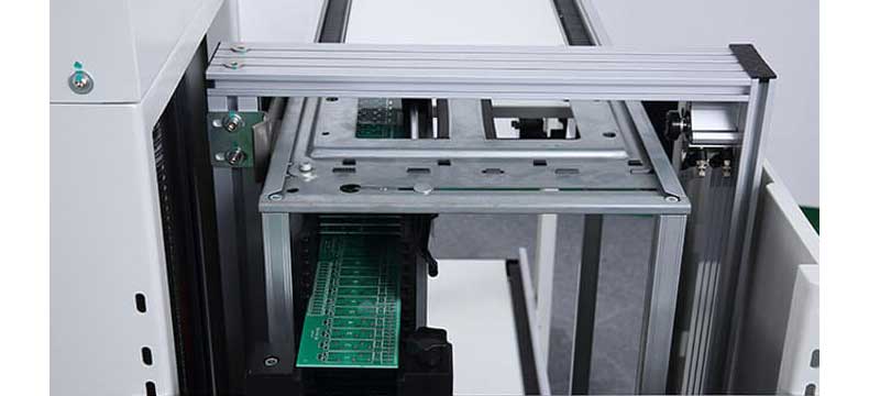
Step 2. Transferring PCBs from automatic loader to solder paste printing machine
When bare PCB boards made at our PCB production basements or sent from customers are brought to our PCBA factory, they are loaded on the automatic loader. Then the loader will transfer the PCBs into the solder paste printing machine.
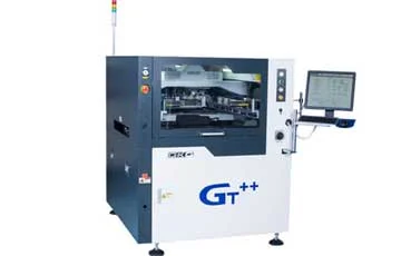
Step 3. Printing solder paste onto the PCBs
Inside the automatic solder paste printing machine, a customized SMT stencil is pre-set. Every PCB board is piled under the SMT stencil, and the scraper blade of the machine will print solder paste on pads of PCBs one by one. Normally, in PCBONLINE, we set the pressure by the blade at 3±0.5KG, its tangle of 60°, and its speed at 60±5mm/s. When the PCB is taken off the SMT stencil, the speed is 0.5±0.05mm/s, and the distance between the PCB and the stencil is set to be 1.0-1.5mm. Then the machine cleans the SMT stencil by drying it up.
Note: Under 0°C to 10°C, the solder paste is thick, and only from 22°C to 28°C when the solder paste is pasty can it be printed. If you DIY a PCBA, please keep your solder paste in the environment under 22°C to 28°C. At PCBONLINE, we store solder paste under 2° to C8°C in the cooler, and before using it for SMT assembly, we take it out and let it stand still for four hours to allow a gentle rise in temperature to 22°C to 28°C.
Step 4. Testing thickness and shape of solder paste
Standard solder paste thickness ranges from 0.09mm to 0.15mm, and the SMT stencil thickness has to be within the tolerance of ±0.03mm than the solder paste thickness. We use the SPI machine to inspect solder paste, and only if its thickness is in this range and its shape is qualified can we let the PCBs go to the next procedure. Some PCBs may require thinner or thicker solder paste, depending on the application requirements, and we will set the custom thickness range.
Step 5. Transferring components into the two mounters
While printing solder paste, we transfer electronic components into high-speed and functional mounters. Small components such as diodes, triodes, resistors, capacitors, inductors, ICs, FPC connectors, and so on, are transferred into the high-speed mounter; large components such as BGAs, FPGAs, USB connectors, connectors, and so on, are transferred into the functional mounter. The components are placed on rolls of tapes on the feeder, and when tapes are pulled by a wheel, components are extracted from the tapes and go into the mounter at their place precisely.
Step 6. Placing small components onto the PCBs
At this step, PCBs printed with solder paste are sent inside the high-speed mounter, and then small components are placed onto the corresponding pads of PCBs. The high-speed mounter runs extremely fast, and in seconds the PCBs are brought next into the functional mounter.
Step 7. Placing large components onto the PCBs
When PCBs mounted with small components come into the functional mounter, large components are placed onto them accurately.
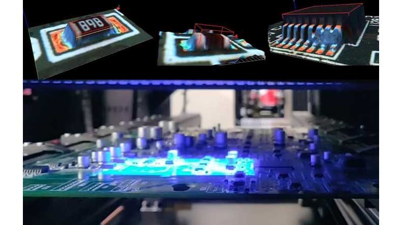
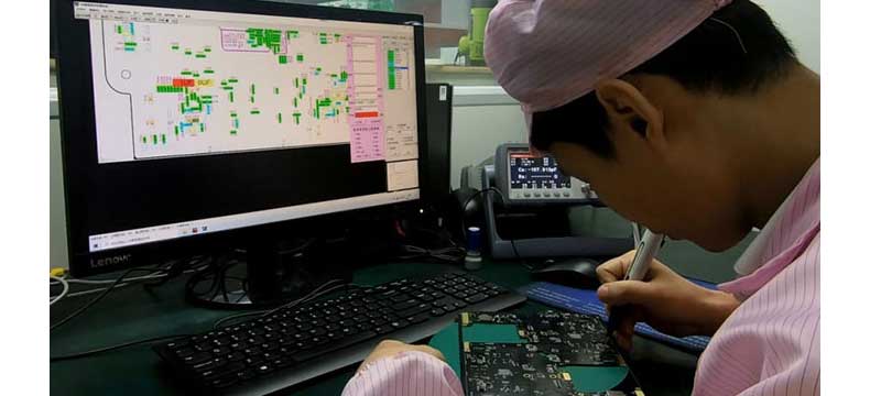
Step 8. X-ray inspection and visual inspection
The mounted PCBs will be transferred into an X-ray machine to detect if there are any soldering defects, and then an experienced technician will inspect some samples visually. The PCBs won’t go to the next step until everything is okay.
Step 9. Reflow soldering
Reflow soldering is the most important step in a PCBA process. Your mounted PCBs are transferred by a conveyor belt moving horizontally with a uniform velocity through a reflowing oven. The reflowing oven has ten temperature zones. From the first to the ninth, temperature increases following the pre-set temperature curve, and solder paste melts on the pads. The tenth is a cooling zone, where solder paste sets. Then electronic components and pads on PCBs are connected tightly, and you are getting the PCBAs.
Note: The velocity of the conveyor and temperatures of the zones of the reflowing oven are not settled. They are set by experienced engineers in our PCBA factory, according to the application requirements. The melting point of the solder paste is 217°C.
Step 10. Repeat step 2 to step 9 to mount components on the other side (optional)
After the above steps, your PCBs are mounted with components on one side, and usually, they will go to the next step. However, some PCBs are designed to have two sides mounted with components. In this case, we will repeat steps from 2 to 9 to mount components on the other side.
Step 11. AOI testing, visual inspection, and sampling inspection
Unlike other PCB assemblers whose AOI is only 2D-scanning, we use 3D-scanning. Any possible defects are noted on the screen, and our AOI operator checks them one by one and records if there are any real defects. The defective products will be picked out. Then another technician checks the PCBAs visually, and the samely, any defects will be recorded, and defective products will be picked out. Next, some PCBA samples will go through the sampling inspection in the testing area. All the defective products will be sent to be repaired, and after repair, they will still be separated from other PCBAs.
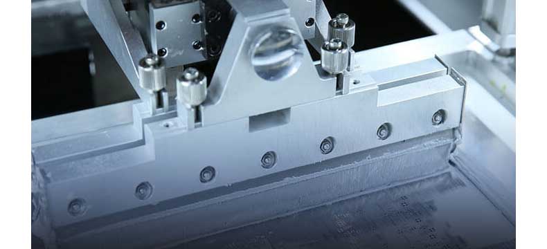
Step 12. Fit long legs of components through PCB holes using DIP
Some components with long legs can't be soldered on PCBs on an SMT assembly line, so the PCBAs are transferred to a THT (through-hole technology) assembly line. We use a DIP machine to insert the long legs through the holes of PCBs.
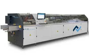
Step 13. Wave soldering
The long legs of components need to be soldered, and wave soldering is processed with two aims: fixing the components with PCBAs and using tin to fill the gap between long legs and PCBA holes to connect components electrically. The soldering side of PCBAs will soak in melting tin through the wave soldering oven, and then, we will use a cutter to trim the component legs to be 1mm to 2mm.
Step 14. Touch-up, cleaning, and visual inspection
After the wave soldering, there may be some defects such as soldering holes and insufficient tin plating, so we need to fix them by touch-up. A well-trained technician inspects the PCBAs carefully and uses a soldering iron to fill the board surface with tin. After this, if there is extra tin on the board, the technician will use flux to remove it in case of a short circuit. Then, the technician inspects the PCBAs again.
Now, the PCBA manufacturing finishes. If customers do not require functional tests, we will bring the PCBAs to the IPQC (in-process quality control) working area, where technicians inspect the PCBAs visually again and then package them. If customers require functional tests, we will process the next procedures.
PCBA Value-Added and Testing
In the post-PCBA process, PCBONLINE can provide various of PCBA value-added services and testing/inspections to ensure the 100% success of PCBA manufacturing, longer PCBA lifespan, and excellent performance and create the final products or systems.
IC programming
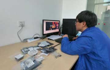
IC programming means downloading programs into integrated circuits. Sometimes, the ICs sent from customers are already downloaded with their own programs, and we will pass this step. A technician connects the IC connector to the computer using a USB cable and clicks the download button to install programs on the IC.
Functional testing using a PCB tester
A technician fits the PCBA on a PCB tester, powers it on, and checks the current, voltage, and other parameters depending on the application use. If the product has a screen, he/she will also check the screen brightness and whether there is flickering and flashing.
Aging testing
Aging tests mean we power the PCBA/product on to let it work at room temperature and a constant higher or lower temperature for a period (usually 12 hours respectively) and then inspect whether the PCBA/product is in good condition. If the PCBA works normally after the aging test, we assemble the product.
Conformal coating
Conformal coating is a urethane/polyurethane coating sprayed on the PCBA surface and baked to cure. It protects the PCBA from moisture, dust, chemicals, vibrations, temperature shocks, etc so that it lengthens the lifespan of the PCBA. It is used in high-end PCBAs such as aerospace PCB assembly.
Box-build assembly
PCBA box-build assembly refers to creating the final products or modules by further processing the PCBA, such as cell contact system assembly, and installing the enclosure to the PCBA.
Not only the above PCBA value-added services and testing, but the one-stop PCB assembler PCBONLINE also provides more inspections such as the application simulation test, tension inspection, environmental test, salt spray test, metallographic inspection, impedance test, etc, according to the PCBA and final product requirements.
Finally, we package the PCBA or products according to the client's requirements and send them to our warehouse, where the products are stored temporarily and delivered to our customers around the globe.
Printed Circuit Board Assembly Capabilities
Applications of PCBA Manufacturing:
R&D and electronic contract manufacturing for consumer electronic products such as projectors, home appliances, Bluetooth headsets, etc.PCBA box-builds for computer and communication electronic products, such as servers, wireless routers, Wi-Fi modules, etc.Manufacturing of industrial and security electronic products, such as industrial controls, HD cameras, face identification cards, smart door locks, etc.PCB assembly for high-end electronic applications for automotive, military, aerospace, and medical industries, such as lithium battery cell contact systems, etc.
GET A FREE QUOTE
PCB and PCBA Certifications


Contact Our Expert Team Now

Learn about our products


Get customized services

 Phone
Phone WhatsApp
 Email
Email
Offer Electronics Manufacturing All-in-One
PCBONLINE® is a registered trademark or service mark of pcb online limited or its affiliates.
Copyright © 2005-2025 Pcb Online Limited. All rights reserved


