
In the field of electronic manufacturing, many people often confuse the concepts of SMD and SMT. This blog will help you understand what SMD and SMT are and how to choose in electronic manufacturing.
In this article:
Part 1. What are Aluminum Core PCBs? Part 2. Aluminum PCBs Composition Part 3. Advantages of Aluminum Core PCBs Part 4. Manufacturing Process of Aluminum Core PCBsAluminum core PCB is a common type of circuit board. The following will reveal its specific composition, application areas and manufacturing process in detail.
What are Aluminum Core PCBs?
Aluminum core PCB is a type of MCPCB. Its standard material is composed of aluminum core and FR-4, and it has single-layer, double-layer and four-layer. With its excellent heat dissipation performance, mechanical strength and high temperature resistance, it is widely used in high-power and high-heat electronic devices.
Aluminum PCBs Composition
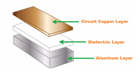
Aluminum core PCB is mainly divided into three layers: conductive layer (circuit layer), insulating layer (dielectric layer), metal base layer (aluminum substrate).
The conductive layer (circuit layer) is mainly composed of electrolytic copper foil, usually with a thickness of 1~35 oz, and 1~4 oz is common.
The base material of the insulating layer (dielectric layer) is high thermal conductivity epoxy resin. However, some high-end aluminum substrates will add ceramic particles (such as aluminum oxide, boron nitride) or polyimide (PI) to improve thermal conductivity.
The material type of the metal base layer (aluminum substrate) is aluminum alloy such as 6061 and 5052, and the thickness ranges from 0.5 to 3.0 mm (commonly 1.0 to 2.0 mm).
Advantages of Aluminum Core PCBs
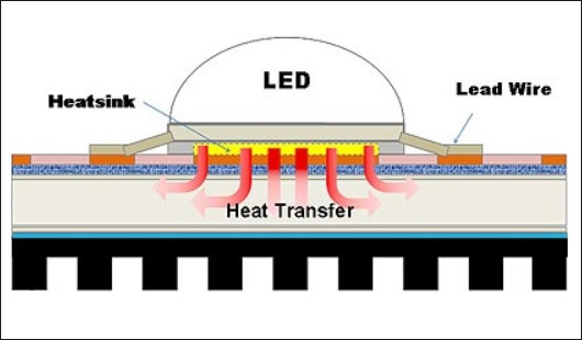
Excellent Thermal Conductivity
One of the most notable benefits of aluminum PCBs is their ability to effectively conduct heat away from critical components. The aluminum core acts as a thermal conductor, dissipating heat much faster than standard materials such as FR4, which helps maintain the stability and performance of electronic devices, especially in high-power applications.
Enhanced Durability and Mechanical Strength
Aluminum PCBs are known for their ruggedness and durability. The metal core not only improves the thermal performance of the board, but it also increases its mechanical strength, making it more resistant to physical stress. This structural integrity ensures that the board can withstand harsher environments, such as high-vibration environments or exposure to extreme temperatures, without compromising performance.
Lightweight and Environmentally Friendly
Despite its strength, aluminum is a lightweight material, which is very useful in applications where weight is a key factor. In addition, aluminum is an environmentally friendly material, and the aluminum base layer and copper foil itself do not contain lead, if the process is proper, because it is non-toxic and recyclable.
Manufacturing Process of Aluminum Core PCBs
1.Substrate Preparation
Select the appropriate aluminum-based material and copper foil thickness and cut it into the required size. Common aluminum-based materials include 5052, 6061 and other aluminum alloys. Different types of aluminum alloys have different mechanical properties and thermal conductivity.
2.Surface Treatment
Surface treatment of the aluminum base to improve its adhesion and corrosion resistance. Common treatment methods include chemical oxidation, passivation, etc.
3.Copper Foil lamination
Copper foil is covered on the aluminum base by rolling or bonding. To ensure good thermal conductivity, it is critical to use a highly thermally conductive insulating dielectric layer.
4.Graphic Transfer
A layer of photosensitive dry film is applied to the copper foil, and then the circuit pattern is transferred to the dry film by exposure and development. This step is like the graphic transfer process of ordinary PCB.
5. Etching
The unprotected copper foil is removed by chemical etching, leaving only the circuit pattern area protected by the dry film. Commonly used etching solutions are ferric chloride or copper sulfate solutions.
6. Film Removal
Use a special solvent to remove the dry film so that the circuit pattern is clearly visible.
7. Drilling and Forming
Drill holes on the aluminum substrate according to the design requirements and perform shape processing. This step requires special attention because the aluminum substrate has high hardness and usually requires the use of special drills and cutting tools.
8. Electroplating
Electroplate on the hole wall and circuit pattern to enhance its conductivity and corrosion resistance. Common electroplating materials include nickel, gold, etc.
9. Solder Mask Coating
Coat a layer of solder mask ink on the circuit pattern and form a solder mask through exposure and development to prevent short circuits during welding. The solder mask can also protect the circuit pattern from the external environment.
10. Silk Screen
Print identification characters, position numbers and other information on the aluminum substrate to facilitate subsequent assembly and debugging.
11. Surface Treatment
Treat the surface of the circuit board, such as tin spraying, gold plating, etc., to improve welding performance and protection performance.
12. Inspection and Testing
Use automatic optical inspection (AOI), X-ray inspection and other means to conduct comprehensive inspection of aluminum substrates to ensure that they meet design requirements and quality standards.
One-Stop HDI PCB Manufacturer and Its PCB Via Filing Capabilities
If you're looking for turnkey HDI electronics manufacturing services (EMS) from hardware development to PCBA fabrication and box-build assembly, you can work with the one-stop HDI PCBA manufacturer PCBONLINE.
Founded in 1999, PCBONLINE has R&D capabilities for HDI projects and EMS manufacturing capabilities, including via filling for stacked vias. It provides 4-to-64-layer HDI PCB fabrication, assembly, and PCBA box-build assembly. You can order various HDI PCBs from PCBONLINE, such as FR4, polyimide (flexible PCB), polyimide + FR4 (rigid-flex PCB), and PTFE/Rogers (high-frequency PCB).

3000m² of production capacity per day for HDI PCBs with builds of 1+N+1, 2+N+2, 3+N+3,4+N+4, and arbitrary interconnection in any layers.
PCBONLINE has hardware and software R&D capabilities for IoT applications requiring HDI design, including PCBA and enclosures.
We can manufacture complex PCBs with stacker vias, via-in-pad, microvias, inlay boards, heavy copper designs, and hybrid and fine structure lay-ups.
Besides HDI PCB fabrication, we have powerful capabilities in fine-pitch assembly for HDI PCB assembly.
We have rich R&D and manufacturing experience for HDI applications such as FPGA boards.
High-quality HDI PCB and PCBA manufacturing certified with ISO 9001:2015, IATF 16949, RoHS, REACH, UL, and IPC-A-610 Class 2/3.
Here'e the PCB via filing capabilities at PCBONLINEL:
- Micriavia filling with copper: laser via size 0.1-0.125mm, priority 0.1mm
- Finished hole size for via-in-pad filling with resin: 0.1-0.9mm (drill size 0.15-1.0mm), 0.3-0.55mm normal (drill size 0.4-0.65mm)
- Max aspect ratio for via-in-pad filling with resin PCB - 12: 1
- Min resin plugged PCB thickness: 0.2mm
- Max via-filling ith resin PCB thickness: 3.2mm
- Making different hole sizes with via filling in one board: Yes
- Via filling with copper/silver: Yes
If you need HDI PCBAs or any other PCBAs requiring via filling, please send your email to PCBONLINE at info@pcbonline.com. We will provide one-on-one engineering support to you.
Conclusion
Via filling is used for creating stacked vias in HDI PCB fabrication, BGA/CSP/QFN IC packaging, and filling PCB via-in-pad with resin during multilayer PCB fabrication. If you need one-stop electronics manufacturing for your HDI PCBA project, contact the one-stop advanced PCB manufacturer PCBONLINE for high-quality PCBA and box-build solutions tailored to your project's needs.
PCB fabrication at PCBONLINE.pdf


