
In the field of electronic manufacturing, many people often confuse the concepts of SMD and SMT. This blog will help you understand what SMD and SMT are and how to choose in electronic manufacturing.
In this article:
Part 1.PCB Solder Stencil Process? Part 2.Pros and Cons Part 3.PCB Solder Stencil IssuePCB Solder Stencil is a critical tool used to precisely apply solder paste to PCB (Printed Circuit Board) pads, ensuring accuracy and consistency in soldering of Surface Mount Technology (SMT) components.
PCB Solder Stencil Process
1.Design Phase
According to the pad type selection (such as square, round, oval), precision components such as BGA/QFN need chamfer design (such as rounding the four corners of the opening) to prevent solder paste from pulling the tip. The opening size is usually 5%~10% smaller than the pad (such as 1.0mm pad, 0.95mm opening) to avoid solder paste overflow and bridging.
2.PCB stencil Installation and Alignment
Use a clamp or magnetic frame to fix the PCB stencil on the printing machine platform. Align the locating pins (Fiducial Pins) with the PCB reference holes to mechanically position the PCB. Finally, use the camera to identify the reference points (Fiducial Mark) of the PCB and PCB stencil to automatically compensate for the offset.
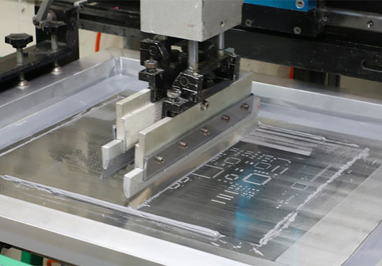
3.Solder Paste Printing
Before use, the solder paste needs to be stirred for 2-3 minutes to restore viscosity and rheology. Then two types of scrapers are used: one is a metal scraper, which is suitable for high-speed printing (such as 60-100 mm/s); the other is a rubber scraper, which has good flexibility and is suitable for uneven PCB surfaces.
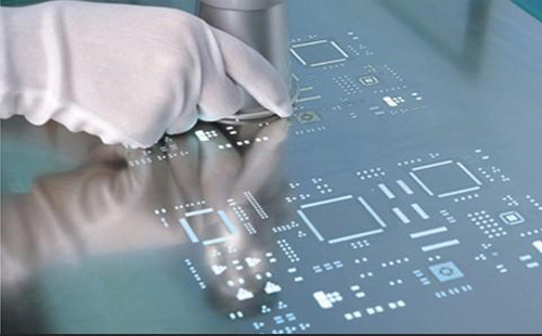
4.Detection and Correction
Use SPI (solder paste detector) to perform laser or structured light scanning to measure the height, volume, and area of solder paste. Data-linked printers automatically adjust scraper pressure or PCB stencil position. Manual inspection: Manually use a magnifying glass or microscope to observe whether the solder paste is uniform, whether there is bridging or contamination, or use a dust-free cloth dipped in alcohol to partially clean the offset or contaminated pads and reprint.
5.PCB stencil Cleaning and Maintenance
First, use a vacuum nozzle to remove the residual solder paste on the surface of the PCB stencil by dry cleaning. Then spray cleaning agent (such as alcohol or deionized water) + ultrasonic oscillation (frequency 40kHz) to deeply clean the opening.
Pros and Cons
Pros
1.High Precision and Consistency
The opening accuracy of laser-cut or electroformed PCB stencil can reach ±5~25μm, which is suitable for micro-pitch components such as BGA and QFN. Through the PCB stencil opening design (such as stepped PCB stencil), the volume of solder paste can be accurately controlled to reduce welding defects (such as cold solder joints and bridging).
2.High Production Efficiency
The fully automatic printer only takes 3 to 10 seconds for a single print, which is suitable for mass production. The SPI (solder paste detector) and the placement machine are linked to achieving full process automation.
3. Adapt to Complex Design
It supports anti-tin bead grooves, local thickening (step PCB stencil), etc. to meet the needs of high-density PCBs and special-shaped pads.
4.Reusable
Stainless PCB stencil has a long life and can be reused thousands of times under normal maintenance, making it suitable for long-term stable production.
Cons
1.High Initial Cost
High-precision laser or electroformed PCB stenciles are expensive (e.g. laser-cut PCB stenciles are about $100-500 per piece, depending on the manufacturer).
2.Complex Maintenance and Cleaning
High-density PCBs require frequent cleaning of the PCB stencil (e.g., once every 50 pieces), otherwise the openings are easily blocked.
3.Environmental Sensitivity
High temperature or mechanical stress may cause the tension of the PCB stencil to decrease, affecting the printing accuracy.
4.Not Suitable for Special Scenarios
For example, in the manufacturing of flexible PCB (FPC), it is difficult to align the PCB stencil with the flexible substrate, and it is easy to offset.
PCB Solder Stencil Issue
Solder paste stencils are an essential production step in printed circuit board manufacturing because they can accurately and consistently apply solder paste to the pads of surface mount devices to ensure that the SMT process equipped with the placement machine can successfully complete the assembly. However, the production process of solder paste stencils is also prone to various unavoidable errors.
Misalignment
Aperture loss refers to a specific opening (Aperture) on the PCB stencil (Solder Paste Stencil) that is not formed correctly, is accidentally blocked, or is physically damaged during the manufacturing/use process, resulting in the inability of solder paste to be deposited on the PCB pad through the hole.
Extra Aperture/Pinhole
Extra Aperture/Pinhole refers to unintended small holes or openings in a solder paste stencil that are not part of the original design. These defects allow solder paste to deposit on unintended areas of the PCB, leading to potential electrical shorts, solder bridges, or other assembly flaws.
Undersized or Clogged Apertures
To achieve the best solder paste transfer, stencil openings that are smaller than necessary are referred to as undersized apertures. When debris or dried solder paste obstructs the apertures, paste cannot deposit onto PCB pads, resulting in clogged apertures. The quality of the solder union is compromised by these problems, which result in irregular or inadequate solder paste volume.
The above is the process and related matters of PCB stencil manufacturing. Most PCB manufacturers are equipped with PCB stencil in-house production, so there is no need to worry about purchasing it separately.
One-Stop HDI PCB Manufacturer and Its PCB Via Filing Capabilities
If you're looking for turnkey HDI electronics manufacturing services (EMS) from hardware development to PCBA fabrication and box-build assembly, you can work with the one-stop HDI PCBA manufacturer PCBONLINE.
Founded in 1999, PCBONLINE has R&D capabilities for HDI projects and EMS manufacturing capabilities, including via filling for stacked vias. It provides 4-to-64-layer HDI PCB fabrication, assembly, and PCBA box-build assembly. You can order various HDI PCBs from PCBONLINE, such as FR4, polyimide (flexible PCB), polyimide + FR4 (rigid-flex PCB), and PTFE/Rogers (high-frequency PCB).

3000m² of production capacity per day for HDI PCBs with builds of 1+N+1, 2+N+2, 3+N+3,4+N+4, and arbitrary interconnection in any layers.
PCBONLINE has hardware and software R&D capabilities for IoT applications requiring HDI design, including PCBA and enclosures.
We can manufacture complex PCBs with stacker vias, via-in-pad, microvias, inlay boards, heavy copper designs, and hybrid and fine structure lay-ups.
Besides HDI PCB fabrication, we have powerful capabilities in fine-pitch assembly for HDI PCB assembly.
We have rich R&D and manufacturing experience for HDI applications such as FPGA boards.
High-quality HDI PCB and PCBA manufacturing certified with ISO 9001:2015, IATF 16949, RoHS, REACH, UL, and IPC-A-610 Class 2/3.
Here'e the PCB via filing capabilities at PCBONLINEL:
- Micriavia filling with copper: laser via size 0.1-0.125mm, priority 0.1mm
- Finished hole size for via-in-pad filling with resin: 0.1-0.9mm (drill size 0.15-1.0mm), 0.3-0.55mm normal (drill size 0.4-0.65mm)
- Max aspect ratio for via-in-pad filling with resin PCB - 12: 1
- Min resin plugged PCB thickness: 0.2mm
- Max via-filling ith resin PCB thickness: 3.2mm
- Making different hole sizes with via filling in one board: Yes
- Via filling with copper/silver: Yes
If you need HDI PCBAs or any other PCBAs requiring via filling, please send your email to PCBONLINE at info@pcbonline.com. We will provide one-on-one engineering support to you.
Conclusion
Via filling is used for creating stacked vias in HDI PCB fabrication, BGA/CSP/QFN IC packaging, and filling PCB via-in-pad with resin during multilayer PCB fabrication. If you need one-stop electronics manufacturing for your HDI PCBA project, contact the one-stop advanced PCB manufacturer PCBONLINE for high-quality PCBA and box-build solutions tailored to your project's needs.
PCB fabrication at PCBONLINE.pdf


