
In the field of electronic manufacturing, many people often confuse the concepts of SMD and SMT. This blog will help you understand what SMD and SMT are and how to choose in electronic manufacturing.
In this article:
Part 1. What are the Surface Mounted Devices (SMDs)? Part 2. What is Surface Mount Technology (SMT)? 3. What are the common SMDs? Part 4. SMT Process StepsWhat are the Surface Mounted Devices (SMDs)?
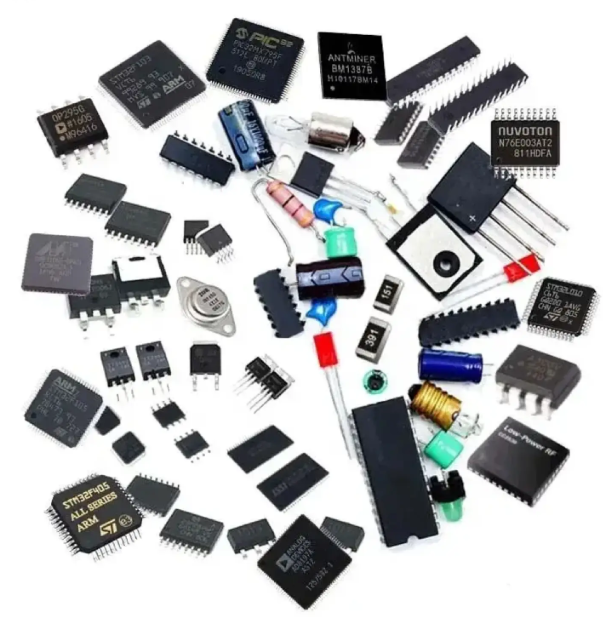
SMDs(Surface Mounted Devices) are electronic components designed for surface mounting. Like chip resistors, chip capacitors, QFP chips, BGA packaging components, etc., they are a special type of component that needs to be soldered on the circuit board to function, which is different from another kind of DIP component (i.e., a plug-in component).
Unlike traditional components, which require wires to be inserted into holes drilled on a printed circuit board, SMDs do not require wires to be inserted into holes, thus simplifying the assembly process and improving efficiency.
What is Surface Mount Technology (SMT)?
SMT(Surface Mount Technology) refers to a production process technology that is used to quickly and accurately mount SMD components on the PCB surface and complete soldering through processes such as reflow soldering.
Process: solder paste printing → component mounting → reflow soldering → inspection.
Core Differences:
Comparison Items |
SMD |
SMT |
Definition |
Specific electronic components |
Production technology |
Use |
PCB functional unit |
Efficient, compact assembly process |
Connection |
Installation by SMT technology |
SMD as processing object |
Example |
SMD LED, SOP package chip |
SMT machine, reflow oven, solder paste |
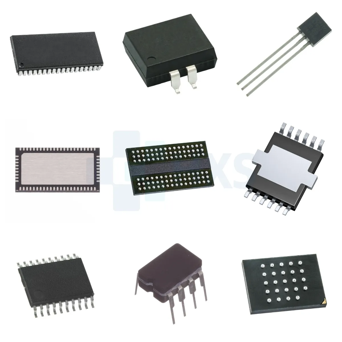
What are the common SMDs?
There are many types of SMD (Surface Mount Device) components, which can be classified from different angles. For example, they can be divided into passive and active components according to their functions; they can be divided into chip components, transistors (SOT), and integrated circuits (IC) according to the packaging form; they can be divided into L-shaped pins such as SOIC, QFP, J-shaped pins, and leadless packages (BGA) according to the pin shape.
To have a more intuitive understanding of the types of SMD components, we use pictures to show some common types:
Chip components (Chip):
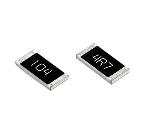
1. Resistors:
Function: Limit the current in the circuit. The larger the resistance value, the smaller the current.
Features: Used for voltage division, current limiting, circuit protection, etc. Accuracy and stability vary depending on materials and processes. The smaller the size, the lower the power handling capacity.
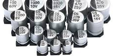
2. Capacitor:
Function: Stores charge and block direct current from passing through, allowing alternating current to pass through.
Features: Used for filtering, coupling, decoupling, energy storage, etc. Capacitance, withstand voltage and temperature characteristics are critical parameters. Capacitors with different dielectric materials have different characteristics.
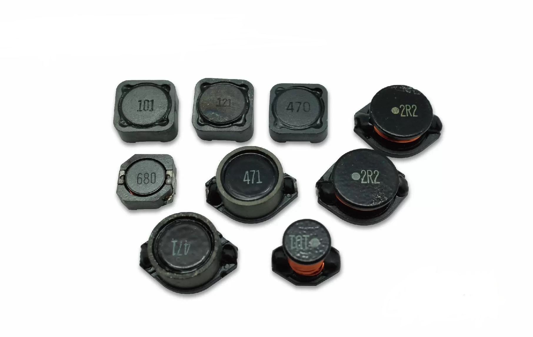
3. Inductor:
Function:
Stores magnetic field and can block AC and allow DC to pass.
Features: Used for filtering, oscillation, choke, etc. Inductance-rated current and quality factors are important parameters. When used in high-frequency circuits, the self-resonant frequency needs to be considered.
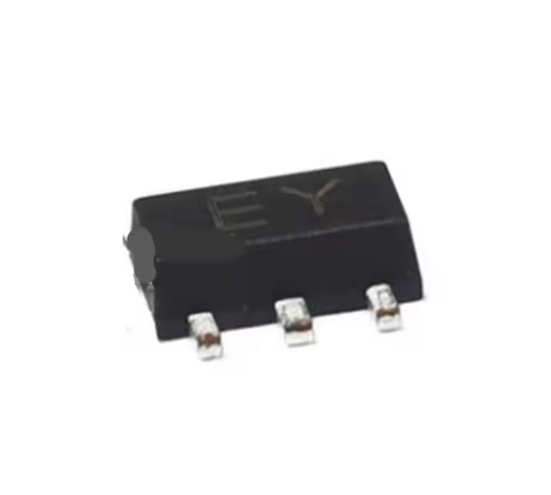
Transistor (SOT):
Small Outline Transistor (SOT):
Function: Amplify or switch electrical signals.
Features: Divided into bipolar transistor (BJT) and field effect transistor (FET). BJT controls collector current through base current. FET controls drain current through gate voltage. Widely used in amplifiers, switching circuits, voltage regulator circuits, etc
Integrated Circuit (IC):
Small Outline Integrated Circuit (SOIC):
Features: Miniaturization: SOIC package is smaller than traditional DIP package and is suitable for high-density circuit boards. Surface Mount: Facilitates automated production and improves production efficiency. Multi-function: Many transistors, resistors, capacitors and other components are integrated internally to achieve complex circuit functions.
Quad Flat Package (QFP):
Features: High Pin Count: The QFP package has many pins and is suitable for complex integrated circuits.
Fine Pitch: The pin pitch is small, which further increases the package density. Surface Mount: Also suitable for automated production
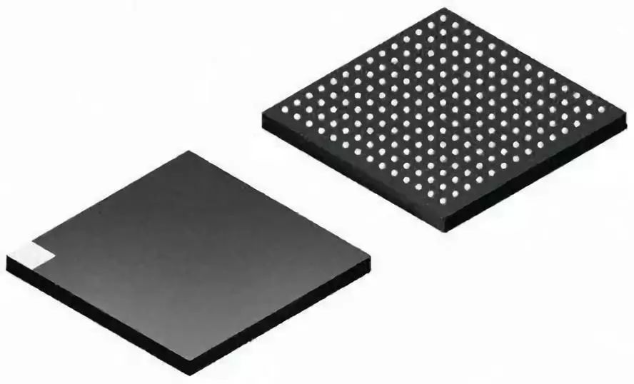
Ball Grid Array Package (BGA):
Features:
High Density: The pins of the BGA package are located at the bottom of the package, which significantly increases the pin density. Good heat dissipation: Spherical solder joints help dissipate heat. High Reliability: The solder joints are strong and have strong vibration resistance. Suitable for high-frequency circuits
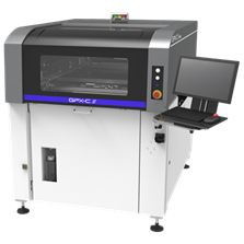
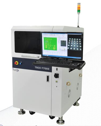
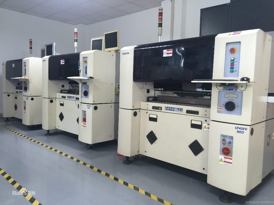
SMT Process Steps
SMT is a complete technical system, including equipment (chip mounter, reflow oven), process (solder paste printing, mounting, welding) and standards (such as IPC specifications), which is used to process SMD components efficiently and accurately. SMD is the processing object of SMT, and SMT is the assembly method of SMD; both are indispensable.
The following are examples of specific SMT processes:
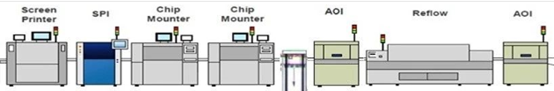
Screen Printer: The process begins with the "Screen Printer," where solder paste is applied to the printed circuit board (PCB) using a stencil. This ensures precise placement of solder paste on the designated pads.
Solder Paste Inspection (SPI): Following the screen printing, the "Solder Paste Inspection (SPI)" stage verifies the quality and accuracy of the solder paste application. This step ensures that the correct amount of solder paste has been applied to each pad. Chip Placement:
Next, the "Chip Placement" machine precisely places small surface mount devices (SMDs), such as resistors and capacitors, onto the PCB.
#1 IC Placement: This step is the first stage of the IC (Integrated Circuit) placement. Where the first set of ICs are placed onto the PCB.
#2 IC Placement: This step is the second stage of the IC placement. Where the second set of ICs are placed onto the PCB.
Automatic Optical Inspection (AOI): After component placement, the "Automatic Optical Inspection (AOI)" system examines the PCB for any placement errors, such as misaligned or missing components.
Reflow Process Inspection (RPI): This is an inspection of the reflow process. It checks the quality of the soldering after the reflow oven.
Reflow Oven: Finally, the PCB is passed through a "Reflow Oven," where controlled heating melts the solder paste, creating permanent connections between the components and the PCB.
Post-reflow Automatic Optical Inspection (AOl) It is performed after the reflow soldering stage (where components are soldered onto a printed circuit board, or PCB, using heat) to automatically detect defects in the assembled PCBs
The above is a general and detailed explanation of the difference between SMD and SMT. In short, in the rapidly developing electronic world, SMT has become a mature and common process.
One-Stop HDI PCB Manufacturer and Its PCB Via Filing Capabilities
If you're looking for turnkey HDI electronics manufacturing services (EMS) from hardware development to PCBA fabrication and box-build assembly, you can work with the one-stop HDI PCBA manufacturer PCBONLINE.
Founded in 1999, PCBONLINE has R&D capabilities for HDI projects and EMS manufacturing capabilities, including via filling for stacked vias. It provides 4-to-64-layer HDI PCB fabrication, assembly, and PCBA box-build assembly. You can order various HDI PCBs from PCBONLINE, such as FR4, polyimide (flexible PCB), polyimide + FR4 (rigid-flex PCB), and PTFE/Rogers (high-frequency PCB).

3000m² of production capacity per day for HDI PCBs with builds of 1+N+1, 2+N+2, 3+N+3,4+N+4, and arbitrary interconnection in any layers.
PCBONLINE has hardware and software R&D capabilities for IoT applications requiring HDI design, including PCBA and enclosures.
We can manufacture complex PCBs with stacker vias, via-in-pad, microvias, inlay boards, heavy copper designs, and hybrid and fine structure lay-ups.
Besides HDI PCB fabrication, we have powerful capabilities in fine-pitch assembly for HDI PCB assembly.
We have rich R&D and manufacturing experience for HDI applications such as FPGA boards.
High-quality HDI PCB and PCBA manufacturing certified with ISO 9001:2015, IATF 16949, RoHS, REACH, UL, and IPC-A-610 Class 2/3.
Here'e the PCB via filing capabilities at PCBONLINEL:
- Micriavia filling with copper: laser via size 0.1-0.125mm, priority 0.1mm
- Finished hole size for via-in-pad filling with resin: 0.1-0.9mm (drill size 0.15-1.0mm), 0.3-0.55mm normal (drill size 0.4-0.65mm)
- Max aspect ratio for via-in-pad filling with resin PCB - 12: 1
- Min resin plugged PCB thickness: 0.2mm
- Max via-filling ith resin PCB thickness: 3.2mm
- Making different hole sizes with via filling in one board: Yes
- Via filling with copper/silver: Yes
If you need HDI PCBAs or any other PCBAs requiring via filling, please send your email to PCBONLINE at info@pcbonline.com. We will provide one-on-one engineering support to you.
Conclusion
Via filling is used for creating stacked vias in HDI PCB fabrication, BGA/CSP/QFN IC packaging, and filling PCB via-in-pad with resin during multilayer PCB fabrication. If you need one-stop electronics manufacturing for your HDI PCBA project, contact the one-stop advanced PCB manufacturer PCBONLINE for high-quality PCBA and box-build solutions tailored to your project's needs.
PCB fabrication at PCBONLINE.pdf


