
PCB (printed circuit board) assembly is the process of PCB manufacturing, assembling, testing, and conducting value-added services such as IC burn-in programming to create the semi-finished product - PCBA.
For advanced PCB, requirements for the PCB assembly process are custom, such as fine-pitch (≤0.5mm), BGA soldering, PTH (through-hole) assembly, etc. How to ensure the quality of advanced PCB assembly? Explore the challenges in advanced electronic assembly and tips from an experienced PCBA manufacturer PCBONLINE.
Advanced PCB Assembly Tips to Solve Floatation in PTH Assembly
Challenge description:
Component floatation in PTH assembly - Floatation is a common issue in wave soldering during PTH assembly. It leads to gaps and uneven surfaces between components and the PCB. This problem arises from improper manual component placement and the thermal expansion of solder paste during reflow.
How to solve the floatation issue and ensure the PTH PCB assembly quality? Below are PCBONLINE's solutions.
Advanced PCB assembly tips:
- When designing the jig/fixture for wave soldering, ensure it not only secures components from high temperatures but also presses down on components vulnerable to move to stop displacement during wave soldering.
- For components requiring high positional accuracy (such as buttons or sockets that must align exactly with the enclosure), use a layer of adhesive to the component bottom before wave soldering. It can effectively minimize deformation. For components prone to movement during reflow soldering, do the same thing.
- Selective soldering is a feasible alternative to prevent soldering defects and component displacement. However, selective soldering has a lower manufacturing efficiency and higher cost than wave soldering. If your advanced PCB assembly project is used for automotive, defense, aerospace, or medical devices, why not consider selective soldering for PTH assembly with no need for the fixtures?
Do you have other solutions to address the floatation issue in PTH assembly? Leave your message in the comments at the end of the article.
Advanced PCB Assembly Tips to Minimize Bubble Rate for BGA PCB Assembly
Challenge description:
BGA is a packaging method for FPGA (field-programmable gate array) chips. Its solder balls are arranged in a grid shape at the bottom of the chip package.
During the SMT production process, after the solder paste melts and solidifies on the BGA pad, it's inevitable to form a certain proportion of bubbles. These bubbles can reduce the mechanical strength of the solder joints, increase the risk of short circuits, and potentially affect electrical connections. According to IPC standards, any solder voids larger than 25% of the BGA pad inspection area are considered defects. Additionally, if the bubble rate exceeds 10%, it can impact the reliability and performance of the entire component.
PCBONLINE's BGA welding quality control standard is to control the bubble rate below 5% to ensure welding quality and final product performance. Below are the tips to control the bubble rate in BGA PCB assembly.
Advanced PCB assembly tips:
- Intelligent data collector/intelligent wearable
- Design a proper reflow profile and control the oven temperatures to reduce the bubble voids. The bubbles form because some air and flux remain in the solder before they can evaporate. So we make a balance between insufficient baking and overbaking by setting up a proper reflow profile in the prototyping testing stage.
- Ensure the metal composition of the solder paste used in PCB assembly is as close as possible to the BGA solder balls.
- X-ray inspection is necessary to inspect the BGA PCB assembly quality. 3D X-ray is better.
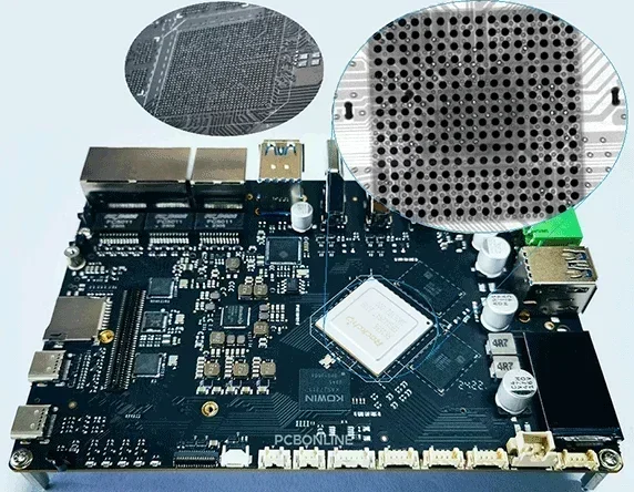
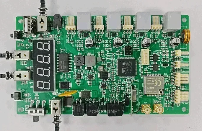
As shown in the picture, it is an RK3588 control board we fabricated and assembled. The bubble rate of the BGA is less than 3%. A low bubble rate in BGA PCB assembly requires advanced production capabilities, precise equipment, and the expertise of our engineers.
Advanced PCB Assembly Tips in SMT Stencils to Prevent Solder Beads and Insufficient Welding
Challenge description:
In advanced PCB assembly, the issues of insufficient welding and solder beads outside the PCB pads may happen. They arise from inappropriate SMT stencil design.
You may wonder - does the PCBA manufacturer not design the holes of the SMT stencil to be 1:1 the same as the PCB pads? Yes, an inexperienced PCBA manufacturer will do that.
Believe it or not, designing the holes of the SMT stencil to be the same as the PCB pads causes solder beads and insufficient welding.
Why? Please see the situations and reasons:
1. For ICs with long and narrow-width leads, such as QFP (quad flat package), the phenomenon of stress concentration will cause the solder paste to shrink. If the SMT stencil holes are the same as the long and narrow-width IC PCB pads, insufficient welding happens because the solder paste on the PCB pad concentrates to the middle.
2. For BGAs and 0402 and 0201-footprint components, stress concentration will also cause the solder paste to shrink to the middle.
![]()
3. For ICs in the leadless packages including QFN (Quad Flat No-lead) LGA (Land Grid Array) and DFN (Quad Flat No-lead), their pads are right-angle on the bottom and at the corners of the package. During PCB assembly, insufficient soldering may happen because the solder can't reach the height of the pad due to stress concentration.
4. For the grounding pads of USB, Mini USB, CF (CompactFlash)/SD (secure digital) cards, both insufficient welding and solder beads may happen.
5. If the grounding pad of the DFN (quad flat no-lead) IC has cross-shaped groves in the center, the metal powders in the solder paste may remain between the cross and pad edges and form solder beads after reflow soldering.
How does PCBONLINE prevent insufficient welding and solder beads? We prevent them by designing the SMT stencils to leave more space for solder paste printing and leave enough space for no solder beads. Please see our tips below.
Advanced PCB assembly tips:
- For ICs with long and narrow-width leads, design the corresponding holes in the SMT stencil to have two round-corner ends to prevent insufficient soldering.
- Design the holes in the SMT stencil for BGA pads and 0402 and 0201-footprint SMDs to be square-shaped to prevent insufficient soldering.
- For IC's right-angle pads on the bottom and at the corner of the package, extend the length of the corresponding holes in the SMT stencil. It allows the solder to "climb" to the height of the IC pads to ensure solder fullness and soldering reliability.
- Increase the solder amount for the grounding pads of USB, Mini USB, and CF/SD cards by designing the SMT stencil hole length 1.2: 1 according to their original pad length. Meanwhile, make the stencil step-down to reduce stress concentration and prevent solder beads.
- For the grounding pad of the QFN, leave a 0.5mm+ space between its cross and the pad edge to prevent solder beads.
- Besides, ensure the SMT stencil holes should be wide enough for at least 4 solder powders to pass through.
Advanced PCB assembly feature demanding requirements for the PCBA manufacturer. If your PCB board has any BGA, leadless package IC, 0402/0201 footprint SMD, IC with long and narrow-width leads, ground pad with cross-shaped groves, or requires a large area of PTH assembly, you will need a professional PCBA manufacturer to provide high-quality PCB assembly and solve all issues for your project.
Advanced PCB Assembly Manufacturer at One Stop
PCBONLINE is a one-stop advanced PCB assembly manufacturer founded in 1999. It has two large advanced PCB manufacturing bases, one PCB assembly factory, stable supply chains, and an R&D team. It focuses on advanced PCB manufacturing and assembly, and you can rest assured of the advanced PCB assembly quality at PCBONLINE, as we provide free DFM (design for manufacturing) and one-on-one engineering support throughout your PCBA project.

PCBONLINE provides free DFM before and during PCBA prototyping, including Gerber/BOM/enclosure checks, manufacturing and testing process design, solving technical and unexpected issues, and selecting affordable alternate components with the same functions and certificates to replace the expensive ones.
PCBONLINE pays attention to SMT stencil and jig/fixture design and temperature control of reflow and wave ovens to ensure full and reliable soldering.
Comprehensive PCBA value-added services and testing in the post-assembly stage, including functional testing, IC burn-in programming, conformal coating, thermal aging, final product box-build assembly, and application simulation testing.
Powerful PCBA manufacturing capabilities, including PCB fabrication of any advanced PCBs, 0.35mm fine-pitch PCB assembly, 3D X-ray inspection, nitrogen reflow soldering, selective soldering, and ability to solve all issues and ensure manufacturing success.
High-quality advanced PCB assembly meeting industrial-grade, medical-grade, automotive-grade, and aerospace-grade requirements. Certified with ISO 9001:2015, IATF 16949:2016, RoHS, REACH, UL, and IPC-A-610 Class 3.
Besides, PCBONLINE can do the R&D for your project or take part in co-development with you. It can prevent unexpected issues in the FAE (field application engineering) stage. To get a quote for your advanced PCB assembly project, email info@pcbonline.com.
Conclusion
Advanced PCB assembly is custom and can encounter various issues in the PCBA manufacturing process. It requires the expertise and experience of the PCB assembly manufacturer to ensure product quality and reliability. This blog demonstrates the challenges and PCBONLINE's tips to solve them. If you need advanced PCB assembly, work with the one-stop PCBA manufacturer PCBONLINE, which will meet your product manufacturing demands and lead to your project's success.
PCB assembly at PCBONLINE.pdf


