
As AI is used widely, AI-powered large language models are implemented in electronic devices or end terminals. To develop AIoT terminals under your brand, you need to design AIoT PCBAs, which are the foundation of electronic devices.
This article will guide you in AIoT device PCBA design and inspire you through an AIoT project example - an AI-powered environmental monitoring sensor. Hoping the content below can help you kickstart your AIoT device project!
In this article:
Part 1. Artificial Internet of Things Devices and Their AIoT PCBAs Part 2. Key Considerations for AIoT PCBA Design Part 3. Project Example: AI-Powered Environmental Monitoring Sensor Part 4. One-Stop PCBA Manufacturer for AIoT DevicesArtificial Internet of Things Devices and Their AIoT PCBAs
Artificial Intelligence of Things (AIoT) combines the technologies of artificial intelligence (AI) with the Internet of Things (IoT).
All IoT terminals, such as smart homes, industrial automation, wearables, and security, come to the era of being powered by AI, which is more data-driven and efficient.
Regarding the development of AIoT devices, there are two ways:
1. Integrating AI algorithms and machine learning directly into the IoT devices.
2. Integrating external services like the open-source large language model DeepSeek API into the IoT devices.
No matter what way you plan to develop your AIoT device, you will need to work on the hardware development. Like any other modern electronic product, the core of AIoT device hardware is their PCBA (printed circuit board assembly).
The PCBA in AIoT devices is a PCB board mounted and embedded with all the electronic components, such as AI chips and accelerators, and provides thermal dissipation.
AIoT PCBAs feature low power consumption (many are battery-powered), high performance, integration of wireless modules, and signal processing. And if the AIoT device has to be designed in a small space, such as the health monitoring wearables, the PCBA has to accommodate a high density of components.
To go forward with the hardware development for your AIoT device, explore the key strategies for AIoT PCBA design below. To illustrate best practices in component selection, PCB layout, and power optimization, there is an AIoT project example: a low-power AI-driven environmental monitoring sensor.
Key Considerations for AIoT PCBA Design
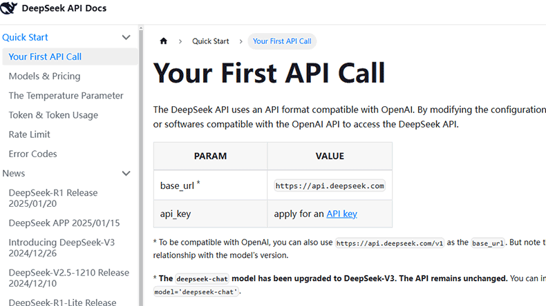
If an engineer wants to develop an AIoT device by integrating the DeepSeek API, the hardware development should focus on the PCBA. This is because the DeepSeek API is accessed through a cloud server, and the PCBA communicates with cthe loud server through a gateway.
Getting the API from https://deepseek.com/api_keys and integrating it with the PCBA is easy: Choosing a proper communication protocol such as HTTP or MQTT to interact with the API. The example codes to apply the API to the device/PCBA can be:
import requests
def call_deepseek_api(data):
url = "https://api.deepseek.com/v1/your_endpoint"
headers = {
"Authorization": "Bearer YOUR_API_KEY",
"Content-Type": "application/json"
}
response = requests.post(url, json=data, headers=headers)
return response.json()
# example for API call
data = {"input": "your_data"}
result = call_deepseek_api(data)
print(result)
The AIoT device development still focuses on their PCBA design. Below are the key considerations for the PCB design.
1. Processor selection: balancing power and performance
Choosing the right AI-capable microcontroller (MCU) or system-on-chip (SoC) is crucial. Options include:
- Edge AI MCUs for ultra-low-power AI inferencing
- NPU-equipped SoCs for handling more complex AI tasks.
- FPGAs for adaptive AI workloads.
Selecting the right processor depends on power constraints, computational needs, and communication capabilities. For battery-powered devices, MCUs with integrated NPUs are ideal, while more complex applications benefit from low-power SoCs with AI acceleration.
2. Efficient power management
AIoT devices often operate on battery or energy harvesting sources, requiring optimized power consumption strategies:
- Dynamic Voltage Scaling (DVS): Adjusting voltage based on computational demand.
- Low-Power Modes: Using sleep and deep-sleep states to minimize energy draw.
- Power-efficient DC-DC converters instead of linear regulators.
- Energy harvesting (solar, piezoelectric, RF energy scavenging) for battery-less operation.
A well-designed power management circuit ensures that AI computations do not significantly drain the battery, making the device suitable for long-term operation.
3. Memory optimization
AI models require RAM for inferencing and Flash for storage. Low-power AIoT designs should:
- Use external QSPI Flash for model storage if internal memory is insufficient.
- Implement memory compression and quantization to reduce footprint.
- Optimize memory access with low-power DRAM.
- Enable caching techniques to reduce repetitive memory reads, lowering power draw.
Choosing the right memory and optimizing access patterns can significantly reduce power consumption in AIoT devices.
4. Wireless connectivity trade-offs
AIoT devices often use Wi-Fi, Bluetooth, LoRa, or NB-IoT for communication. Each has different power implications:
- Bluetooth Low Energy (BLE 5.2+) for intermittent data transmission.
- LoRaWAN for ultra-long-range, low-power networking.
- Wi-Fi 6 with Target Wake Time (TWT) to optimize power consumption.
- NB-IoT for low-bandwidth, cellular-based long-distance communication.
Power-efficient wireless protocols ensure AIoT devices can remain operational for extended periods without frequent battery replacements.
5. Thermal management in compact designs
AI workloads generate heat, impacting performance and longevity. Solutions include:
- Copper pours and thermal vias for efficient heat dissipation.
- Graphene-enhanced thermal pads for compact, fanless designs.
- Power-efficient AI accelerators to reduce unnecessary heat.
- Active cooling (if necessary) using miniature fans or heat pipes.
Project Example: AI-Powered Environmental Monitoring Sensor
To illustrate the above general AIoT PCBA design considerations, let's design an AIoT environmental monitoring PCBA that detects temperature, humidity, and gas detection using an Edge AI model for real-time anomaly detection.
1. Project requirements
This AIoT sensor project aims to monitor environmental parameters efficiently while leveraging edge AI for local data analysis.
The key requirements for the system include:
- Microcontroller: ESP32-S3, selected for its AI acceleration, low power consumption, and built-in Wi-Fi and Bluetooth for easy data transmission.
- Sensors: Temperature, humidity, and gas detection, enabling comprehensive environmental monitoring.
- Communication: LoRa module for long-range data transmission, suitable for remote monitoring applications.
- AI processing: On-device anomaly detection to analyze air pollution trends and detect abnormal conditions in real-time.
The sensor collects environmental data, processes it using an AI model running on the ESP32-S3, and transmits critical alerts or summaries via LoRa. Including edge AI reduces the need for continuous cloud connectivity, minimizing power consumption and improving response times.
2. Schematic design
The schematic design integrates multiple components ensuring efficient power usage and reliable data transmission. The ESP32-S3 serves as the core processing unit capable of handling AI tasks efficiently while supporting low-power operation. The gas sensor, flame sensor and relay module are interfaced via GPIO pins while the temperature and humidity sensor is connected via I2C for real-time environmental monitoring.
- Temperature & humidity sensor: SHT31, connected via I2C, providing accurate environmental readings.
- Gas sensor: MQ-135, used for detecting air quality and pollution levels.
- Flame sensor: LM393 IR-based flame detection for fire hazard monitoring.
For power management, a 5V relay module (SRD-05VDC-SL-C) is used to control power flow. The relay helps cut off power to sensors and peripherals when the device is in deep sleep mode, significantly reducing power consumption.A MOSFET-based power switching circuit ensures smooth transitions between active and low-power states.
The LoRa communication module is connected via SPI, enabling long-range data transmission with minimal power consumption.
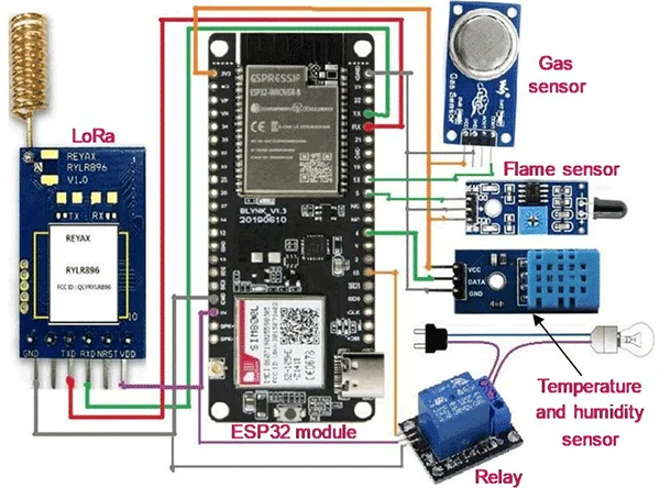
Schematic showing connections between ESP32-S3, sensors, relay, and LoRa module
3. PCB layout optimization
The PCB layout is designed to ensure stable performance, efficient power use, and effective heat management. The ESP32-S3 is placed in the center of the board to keep connections short and reduce signal delays. The LoRa module is positioned at the edge to improve antenna performance and prevent interference from other components.
To maintain a clean and stable signal, a ground plane covers the entire PCB, reducing unwanted electrical noise. Power traces are designed to be short and wide, ensuring smooth power delivery and minimizing energy loss.
For thermal management, thermal vias are placed directly under the ESP32-S3's power regulation IC, voltage regulator, and main processing unit to enhance heat dissipation. Additional vias are positioned near high-current traces and the LoRa module to further improve thermal management. At least 6 thermal vias are strategically placed to aid heat dissipation.
Copper pours are used around power-intensive components to spread heat efficiently.
For noise reduction, high-frequency components, such as the LoRa module and clock oscillators, are isolated to reduce interference.
A dedicated analog ground plane is used for noise-sensitive sensors, preventing signal distortion.
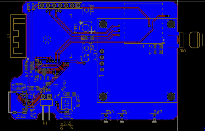
PCB layout of the AIoT sensor
4. Firmware optimization for low power
Key techniques:
- Quantized AI models (using TensorFlow Lite for Microcontrollers) to reduce computational load.
- Adaptive sampling—reducing sensor data frequency during stable conditions.
- Peripheral clock gating—turning off unused modules dynamically.
- Event-driven AI processing—running inference only when environmental changes are detected.
- Sleep scheduling to ensure maximum battery efficiency.
The AI model operates on a threshold-based activation mechanism which can be initiated in the Arduino IDE platform by defining the threshold values of each sensor.
If the MQ-135 gas sensor detects a CO2 concentration above 1000 ppm, the AI model runs an anomaly detection routine and triggers an alert.
Similarly, the flame sensor activates the AI model only when infrared signatures exceed a predefined threshold.
For deep sleep implementation, the ESP32-S3 wakes up every 10 minutes to take sensor readings. If no anomalies are detected, it goes back to deep sleep. If a threshold is exceeded, the AI model processes data and sends an alert.
Here is the Arduino IDE Firmware Code:
#include <Wire.h>
#include "Adafruit_SHT31.h"
#include <LoRa.h>
#include <esp_sleep.h>
#define GAS_SENSOR_PIN 34
#define FLAME_SENSOR_PIN 35
#define TEMP_THRESHOLD 30.0
#define GAS_THRESHOLD 1000
#define FLAME_THRESHOLD 500
#define SLEEP_DURATION 600 // Sleep for 600 seconds (10 minutes)
Adafruit_SHT31 sht31 = Adafruit_SHT31();
void setup() {
Serial.begin(115200);
pinMode(GAS_SENSOR_PIN, INPUT);
pinMode(FLAME_SENSOR_PIN, INPUT);
if (!sht31.begin(0x44)) {
Serial.println("Couldn't find SHT31 sensor!");
}
LoRa.begin(915E6);
}
void loop() {
float temp = sht31.readTemperature();
int gasLevel = analogRead(GAS_SENSOR_PIN);
int flameLevel = analogRead(FLAME_SENSOR_PIN);
bool alertTriggered = false;
if (temp > TEMP_THRESHOLD) {
Serial.println("High temperature detected!");
sendLoRaMessage("Temp Alert: ", temp);
alertTriggered = true;
}
if (gasLevel > GAS_THRESHOLD) {
Serial.println("High gas level detected!");
sendLoRaMessage("Gas Alert: ", gasLevel);
alertTriggered = true;
}
if (flameLevel > FLAME_THRESHOLD) {
Serial.println("Flame detected!");
sendLoRaMessage("Flame Alert!");
alertTriggered = true;
}
if (!alertTriggered) {
Serial.println("No anomalies detected. Entering deep sleep...");
esp_sleep_enable_timer_wakeup(SLEEP_DURATION * 1000000ULL);
esp_deep_sleep_start();
}
delay(5000); // Small delay before next loop iteration
}
void sendLoRaMessage(const char* message, float value = 0) {
LoRa.beginPacket();
LoRa.print(message);
if (value != 0) {
LoRa.print(value);
}
LoRa.endPacket();
}
By employing these optimizations, the AIoT sensor achieves real-time monitoring with minimal power consumption, making it ideal for long-term deployment in remote environments.
5. Final PCB design and 3D visualization
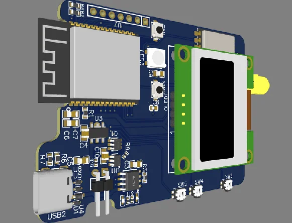
Optimized PCB Design
The PCB layout is designed to ensure stable performance, efficient power use, and effective heat management. The ESP32-S3 is placed in the center of the board to keep connections short and reduce signal delays. The LoRa module is positioned at the edge to improve antenna performance and prevent interference from other components.
Optimizing AIoT PCBs for low power and high performance requires a holistic approach, from hardware selection to firmware tuning. This environmental monitoring project demonstrates how proper component selection, PCB layout techniques, and AI model optimizations can enable efficient AIoT devices.
One-Stop PCBA Manufacturer for AIoT Devices
For those seeking AIoT device hardware development with high performance and low power consumption, PCBONLINE provides tailored R&D and PCBA manufacturing for AIoT applications. Founded in 1999, PCBONLINE has two large advanced PCB manufacturing bases, one PCB assembly factory, stable supply chains, and an R&D team.

PCBONLINE has R&D capabilities and rich AIoT development experience. We can do the R&D or take part in your project's development from the early stages.
PCBONLINE offers free design for manufacturing (DFM) and one-on-one engineering support and solves all technical issues to ensure the smooth manufacturing process and successful results of your AIoT project.
Strong and one-stop automotive and IoT PCBA manufacturing capabilities custom meeting your requirements, including R&D, prototyping/sampling, PCB fabrication, component sourcing, PCB assembly, PCBA value-added, and IoT device box-build assembly.
The automotive industry components that PCBONLINE provides for PCB assembly are reliable and traceable. You can check our PCB certifications, including ISO 9001:2015, IATF 16949:2016, REACH (EC 1907/2006), RoHS (Directive 2002/95/EC), and UL.
As a source factory manufacturer for PCBA and AIoT devices, the electronics manufacturing from PCBONLINE is at reasonable prices without hidden costs.
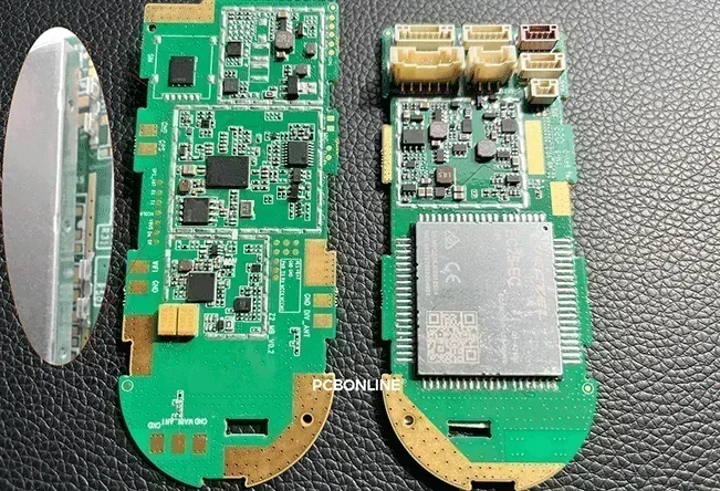
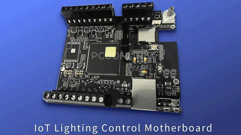
This AIoT motherboard project for shared scooters was not involved in the initial R&D by PCBONLINE, but during our free pre-production DFM process, we helped the client resolve the following issues. We prevented design defects from unnecessary costs and helped the client reduce component procurement costs by at least 10%.
During the DFM review, our engineers discovered that the client's design used a surface-mounted shield cover. This would prevent components beneath the shield from being inspected with AOI and X-ray after SMT assembly. We recommended changing to a snap-on shield, which would allow the shield to be placed after the AOI and X-ray inspections. The client agreed to our suggestion.
In addition, in the DFM inspection, our engineers identified discrepancies between the BOM specifications for three passive components and the PCB design's pad and package. We alerted the client to this issue, and they ultimately modified the PCB pads and layout to resolve this potential risk.
As PCBONLINE consolidates component procurement, we receive significant discounts from brands and distributors, especially for IoT communication modules (for major MCU companies like Espressif and Neoway, we have strategic direct partnerships with the manufacturers). This gives us a large pricing advantage. The client informed us that we helped them save 15% on component procurement costs.
The professional team at PCBONLINE specializes in creating high-quality AIoT PCBs and PCBAs tailored to your project's custom needs. To get a quote for your AIoT device PCBs, please contact info@pcbonline.com.
Conclusion
By implementing best practices in PCB design and optimization, AIoT devices can function efficiently for extended periods without frequent maintenance. Whether it's using dynamic power management techniques, selecting energy-efficient processors or optimizing the PCB layout for thermal performance, every design decision plays a role in ensuring the overall success of an AIoT system. To design and manufacture AIoT PCBs for your project, work with PCBONLINE.
PCB assembly at PCBONLINE.pdf


