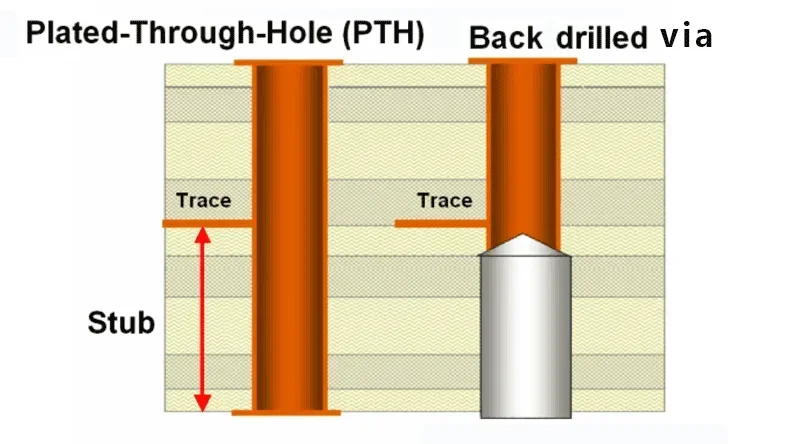
What is back drilling? It is a PCB (printed circuit board) depth-controlled drilling process that removes the unwanted portion of the PTH (plated through-hole). We call the unwanted portion of the PTH "stub".
After the PCB back-drilling process, we get the back-drilled via. It is the entire via structure after the stub has been removed.
As an advanced PCB manufacturer, PCBONLINE can drill microvias (stacked, staggered) and back-drilled vias on HDI PCBs, high-speed PCBs, and high-frequency PCBs as wanted. Below are the back drilling capabilities of PCBONONLINE. You can learn more about PCB back drilling with the figures in the table.
|
Back drilling features
|
PCBONLINE' capabilities |
Figures
|
|
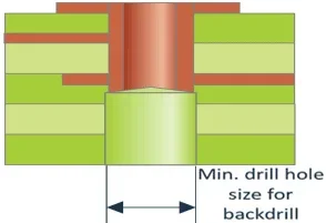
Drill hole size for back drilling
|
0.5mm to 6.2mm
|
 |
|
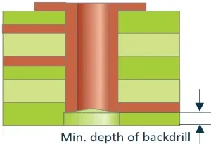
Min. depth of back drilling
|
0.2mm
|
 |
|
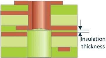
Insulation thickness between back drilling layers
|
≥0.2mm
|
 |
|
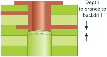
Depth tolerance to back drilling
|
±0.1mm
|
 |
|
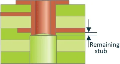
Remaining stub
|
Not defined
|
 |
Now, you know the PCB backfilling capabilities at PCBONLINE. For more details about our PCB manufacturing or having questions about your project, feel free to chat with us from the online chat window.
Why is Back Drilling Needed for High-speed Circuits?
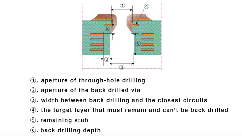
Back drilling is not necessary for all multilayer PCBs but only when the unused portion of the PTH, stub, affects the signal integrity at high speeds and high frequencies.
For high-speed PCBs, high-frequency PCBs, and HDI PCBs, the stub leads to issues of parasitic effects, signal reflection, and impedance discontinuities.
Parasitic capacitance
The stub increases parasitic capacitance. It can change the signal path's intended impedance and cause signal degradation.
In the below table, you can see the capacitance values of the copper-plated vias in different specifications.
|
drill head diameter
|
copper-plated via aperture
|
insulation annular ring outer diameter
|
pad diameter
|
copper-plated via length (mil)
|
copper plated via effective capacitance
|
|
26
|
22
|
52
|
38
|
250
|
2.4
|
|
26
|
22
|
52
|
38
|
200
|
2.0
|
|
26
|
22
|
52
|
38
|
225
|
1.8
|
|
26
|
22
|
52
|
38
|
150
|
1.5
|
|
26
|
22
|
52
|
38
|
125
|
1.3
|
|
26
|
22
|
52
|
38
|
100
|
1.0
|
The via effective capacitance is the parasitic capacitance introduced by the copper-plated via. It should be as small as possible to maintain signal integrity and high-speed signal performance.
The smaller than copper-plated via length, the smaller via effect capacitance. So back drilling is effective in reducing the parasitic effect.
Signal reflection
The stub acts as an open-ended transmission line and reflects signals. At high speeds and high frequencies, it causes signal loss, jitter, and bit errors.
In the below figure, you can see an increased copper-plated via length leads to more signal reflection, and it limits the maximum length of the signal line.
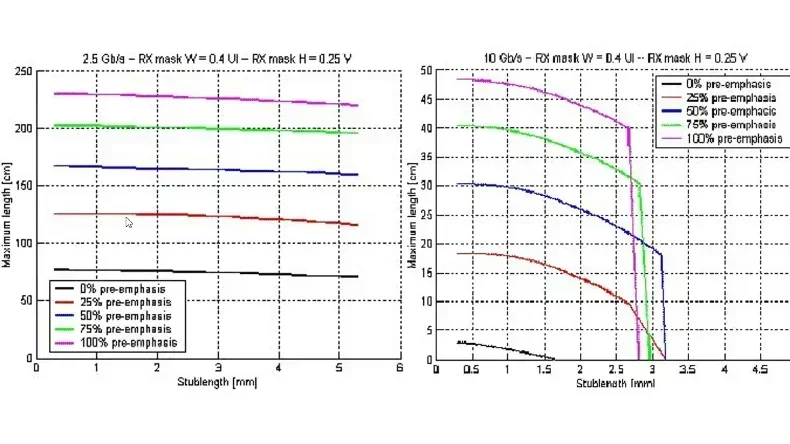
That's why back drilling is needed to control the negative impact of via length on signal lines.
Impedance discontinuities
The inductance (Ls) introduced by the stub causes impedance discontinuities along the signal path. The high-speed signals are sensitive, and the signal discontinuities lead to signal interference.
In the below figure, you can see the influence of Ls on the impedance.
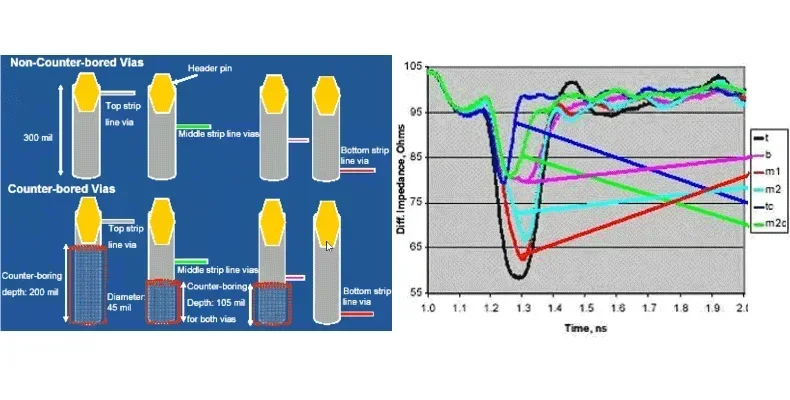
To reduce the influence of Ls on the impedance in high-speed and high-frequency circuits, you should make the PTH via quantity and via length as small as possible, use blind vias and buried vias to reduce the via length along the signal path, and use back drilled via to reduce the Ls.
Overall, by removing the stub, the remaining back drilled via structure can achieve signal integrity. Besides, as you can see from our back drilling specification table, the insulation thickness ensures circuit insulation.
PCB Contract Manufacturer Good at Back Drilling and Impedance Control
To ensure your back-drilled via PCB project's success, you can work with PCBONLINE, an advanced PCB and PCBA manufacturer with R&D and one-stop manufacturing capabilities.
PCBONLINE has two large advanced PCB manufacturing bases, one PCB assembly factory, stable supply chains, and an R&D team to provide PCB contract manufacturing for high-speed and high-frequency devices requiring PCB back drilling.

PCBONLINE has expertise and powerful capabilities in controllable mechanical deep drilling to achieve the required impedance range of the PCB.
Offer various options for back-drilled via PCB manufacturing, including HDI PCBs with arbitrary layer connections, and high-frequency (PTFE) PCBs for automotive, communications, aerospace, and military applications.
PCBONLINE offers free DFM (design for manufacturing) including solving issues before and during the prototyping stage to ensure the success of your high-speed project.
PCBONLINE can provide all R&D for your high-speed project including PCB, PCBA, and enclosures, or take part in co-development with your engineering team.
One-stop back drilled via PCB contract manufacturing, including PCB fabrication, PCB assembly, PCBA value-added services, and box-build assembly from prototypes to mass production.
PCBONLINE will provide one-on-one engineering support no matter the number of boards you want. To get a quote from PCBONLINE, please email info@pcbonline.com.
Conclusion
This blog concisely tells you what PCB drilling is and the reasons for using back-drilled vias in HDI, high-speed, and high-frequency PCBs. PCBONLINE is a one-stop PCB manufacturer for high-speed and high-frequency devices for automotive, communications, aerospace, and military applications. To ensure the success of your project, work with PCBONLINE who can precisely control the via depth and impedance.
PCB assembly at PCBONLINE.pdf


