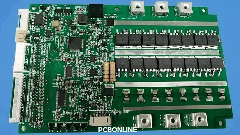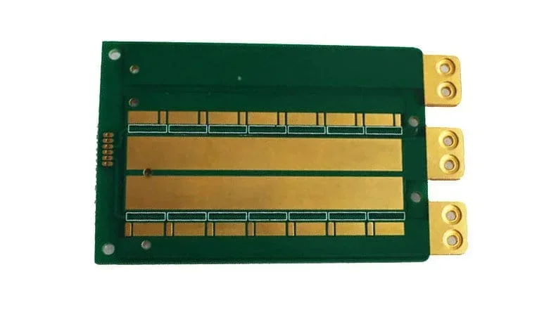
In regular PCB design, the current to flow through the PCB traces are within 10A, 5A, and even 2A, especially for commercial electronics. However, for high-power and high-current devices, such as the battery management system (BMS) for electric vehicles, and industrial inverters, their PCBs require a higher current capacity of the PCB traces. The current capacity of PCB traces for these high-current applications may reach 50A, 80A, 100A, and even 200A.
How to increase the current capacity of PCB traces? Explore tips and solutions from this blog post.
What is the Current Capacity of PCB Traces
First, let's define what the current capacity of PCB trace is. It is the maximum current value that can safely pass through the PCB traces without causing overheating and other issues.
n theory, the formula of the current capacity of PCB traces according to the IPC-2221 standards is:
I=K⋅Wa⋅Hb
Where I stands for the theoretical current capacity of PCB traces in amperes (A),
W is the trace width in mils,
H is the copper thickness in oz,
K, a, and b are empirical coefficients. At a 10°C temperature rise, for external traces, K=0.048, a=0.44, b=0.725, for internal traces, K=0.024, a=0.44, b=0.725. At a 20°C temperature rise, for external traces, K=0.095, a=0.44, b=0.725, for internal traces, K=0.048, a=0.44, b=0.725.
In practice, the current capacity of PCB traces is larger than the above theoretical value, as the high-current PCB design should leave abundance for current capacity.
How to Increase the Current Capacity of PCB Traces

First, let's reveal the 3 tips on how to increase the current capacity of PCB traces:
Increasing copper thickness,
Increasing trace width,
Increasing temperature rise.
Below, you can find a table of the currents that flow through the PCB traces vs the PCB trace widths and copper thicknesses at a 10°C temperature rise.
|
Copper thickness/1oz
|
Copper thickness/2oz
|
Copper thickness/3oz
|
|||
|
Current (A)
|
Trace width (mm)
|
Current (A)
|
Trace width (mm)
|
Current (A)
|
Trace width (mm)
|
|
0.55
|
0.2
|
0.7
|
0.2
|
0.9
|
0.2
|
|
0.8
|
0.3
|
1.1
|
0.3
|
1.3
|
0.3
|
|
1.1
|
0.4
|
1.35
|
0.4
|
1.7
|
0.4
|
|
1.35
|
0.5
|
1.7
|
0.5
|
2
|
0.5l
|
|
1.6
|
0.6
|
1.9
|
0.6
|
2.3
|
0.6
|
|
2
|
0.8
|
2.4
|
0.8
|
2.8
|
0.8
|
|
2.3
|
1
|
2.6
|
1
|
3.2
|
1
|
|
2.7
|
1.2
|
3
|
1.2
|
3.6
|
1.2
|
|
3.2
|
1.5
|
3.5
|
1.5
|
4.2
|
1.5
|
|
4
|
2
|
4.3
|
2.5
|
5.1
|
2
|
|
4.5
|
2.5
|
5.1
|
2.5
|
6
|
2.5
|
How about the different current capacities of PCB traces vs. PCB trace widths and copper thicknesses at a 20°C temperature rise? Please view the table below.
|
Copper thickness/3oz
|
Copper thickness/4oz
|
||
|
Current (A)
|
Trace width (mm)
|
Current (A)
|
Trace width (mm)
|
|
7.2
|
1
|
8.6
|
1
|
|
8.2
|
1.2
|
9.8
|
1.2
|
|
9.6
|
1.5
|
11.5.
|
1.5
|
|
11.8
|
2
|
14.2
|
2
|
|
13.9
|
2.5
|
16.7
|
2.5
|
|
15.9
|
3
|
19.1
|
3
|
|
19.6
|
4
|
23.5
|
4
|
|
23.1
|
5
|
27.7
|
5
|
|
32.4
|
8
|
38.9
|
8
|
|
33.6
|
10
|
45.8
|
10
|
To design a 100A high-current PCB for a 20°C temperature rise, you can choose 4oz copper thickness and 36mm trace width with thermal dissipation settings such as the heat sinks and copper busbars.
If you want to design a 50A high-current PCB for a 20°C temperature rise, you can design a 3oz copper thickness and 15mm trace width or 4oz copper thickness and 11mm trace width for the outer layers. You can design a 4oz copper thickness and 20mm trace width for the inner layers or a 6oz copper thickness and 13mm trace width. Besides, your PCB and product require additional heat dissipation designs including heat sinks, multilayer circuits, and metal enclosures to prevent overheating.
Other Methods for Increasing PCB Current Capacity
Increasing copper thicknesses, and trace widths, and allowing for more temperature rises can increase the current capacity of PCB traces. What are the other methods to increase the current capacity of the PCB?
Below are the methods to improve thermal dissipation so that the larger currents can flow through the PCB:
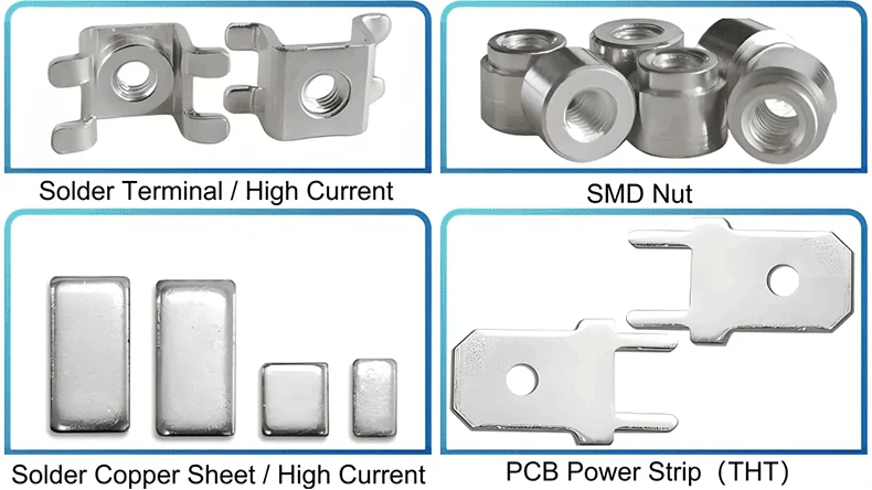
Using terminal connectors — On the PCB or the enclosure, install several terminal connectors that can withstand high currents, such as the SMD nuts, PCB terminals, and copper sheets. Then connect the high-current wires for the high currents to flow through to the terminal connectors.

Using PCB busbars — On the PCB, copper busbars can surface mount at the pins of the component that generate a lot of heat, or they can embed at the bottom of the component for high current conductivity and thermal dissipation. The PCB busbars can be custom-made according to your requirements. Below, you can find the common PCB busbar sizes and the currents to flow through them on the PCB.
|
PCB busbar sizes (mm)
|
Current capacity (A)
|
|
13 x 4 x1
|
30.2
|
|
10 x 5 x1
|
29.1
|
|
11 x 4 x 1
|
25.6
|
|
8 x 5 x 1.8
|
23.3
|
|
6 x 5 x 1
|
17.5
|
|
10 x 3 x 1
|
17.5
|
|
8.5 x 3 x 1
|
14.8
|
|
6 x 4 x 1
|
13.9
|
|
9 x 2 x 1
|
10.5
|
|
4 x 4 x 1.5
|
9.3
|
|
3.5 x 3 x 1
|
6.1
|
|
6 x 3 x 0.3
|
1.05
|
High-current PCBA Manufacturing under One Roof
If you want one-stop electronics manufacturing for your high-current PCB and product project, you can work with the advanced PCBA manufacturer PCBONLINE.

Founded in 1999, PCBONLINE has two large advanced PCB manufacturing bases, one PCB assembly factory, stable supply chains, and an R&D team for high-current PCBA projects.
PCBONLINE fabricates and assembles thick-copper PCBs with copper thickness up to 14oz.
PCBONLINE can do the R&D and complete one-stop electronics manufacturing for your high-current project, including custom busbars, PCBA prototyping, PCB fabrication, component sourcing, PCB assembly, PCBA value-added, and box-build assembly.
PCBONLINE provides free design for manufacturing (DFM) and one-on-one engineering support and solves all technical issues to ensure the smooth process and successful results of your high-current PCBA project.
PCBONLINE has rich experience in jig design and reflow/wave soldering oven temperature controls for high-current PCB assembly.
Besides, it has strategic cooperation with the top 3 mold and enclosure manufacturers in China for the jigs and enclosures used for the high-current PCBA projects.
Reasonable prices without hidden costs for high-current PCBA manufacturing as PCBONLINE is a source factory manufacturer.
High-quality PCBA manufacturing certified with ISO 9001:2015, ISO 14001:2015, IATF 16949:2016, RoHS, REACH, UL, and IPC-A-610 Class 2/3.
PCBONLINE has completed many high-current PCBA projects successfully for our clients, especially the thick-copper ones and those with copper busbars. The applications include the battery management system for battery packs, power equipment, industrial inverters, industrial servo motors, EV charging piles, transformers, etc. To get a quote for your high-current PCBA project, contact info@pcbonline.com.
Conclusion
This blog defines the current capacity of PCB traces and gives tips to increase it by increasing copper thicknesses, trace widths, and temperature rises. Besides, it introduces the other methods for high-current PCBs using terminal connectors and PCB busbars. For high-current PCBs and devices, such as the thick-copper PCBs, and PCBs with copper busbars and terminals, you can work with the one-stop PCBA manufacturer PCBONLINE. If you have any high-current PCB demands or questions, chat with the professionals from PCBONLINE from the online chat window.


