
What are circuit boards' edge connectors? Explore everything about PCB edge connectors easily.
What Are Edge Connectors in Printed Circuit Boards
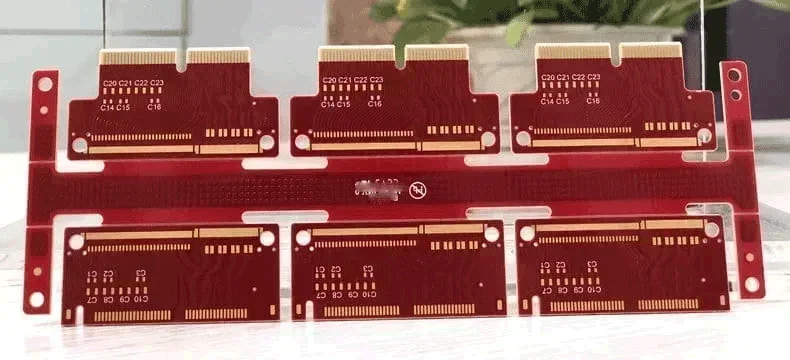
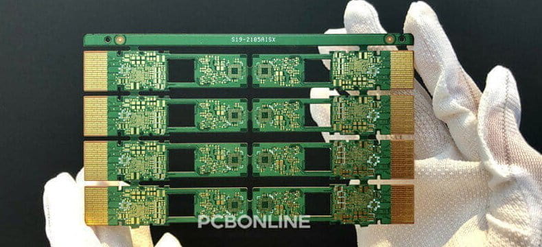
Edge connectors, or PCB gold fingers, are a row of dense hard gold-plated pads on the circuit board edges.
These PCB pads, with excellent wear resistance that can withstand thousands of plug-ins and outs, are used for frequent insertion and removal of the PCB from the motherboard or device.
You can easily distinguish the edge connectors for these features:
- Edge connectors are a series of exposed copper pads without components soldered to them.
- They are on the edge of the PCB for contact with the corresponding connector when the PCB is inserted into it.
- From the appearance, PCB edge connectors are plated with hard gold, so you can find them as a row of bright yellow conductors.
- The exposed FR4 edges of the PCB commonly have a bevel of 20°, 30°, or 45 ° for easy insertion or removal of the PCB.
- Between and near the edge connectors, there should be a clearance area free from components and lines to prevent short circuits.
- A high-temperature tape may be attached to the edge connectors to protect it from thermal damage during reflow soldering.
Specifications of Circuit Board Edge Connectors
What are the critical specifications of edge connectors on circuit boards? Check the clearance ranges, beveling of edge connectors, and gold/nickel thicknesses below.
Clearance Ranges of Circuit Board Edge Connectors
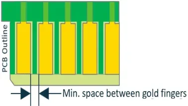
The clearance between and near edge connectors on a circuit board ensures proper fit and electrical isolation.
The clearance between the edge connectors is the space between the adjacent edge connectors. The typical minimum space between the adjacent edge connectors is 0.15mm (6mil).
At the advanced PCB manufacturer PCBONLINE, the minimum space between edge connectors is:
- Dry film pattern plating 0.175mm
- Lead process 0.125mm
The clearance range from the physical edge of the PCB to the edge connector pads is 0.6mm-1.5mm. It prevents damaging the edge connectors when routing the bevels.
The clearance from the edge connector pads to the PTH (plated-though) hole and the other pads (including via pads) should be 1mm and above.
The clearance from the edge connector pads to the circuit traces should be 0.2mm and above.
Beveling of Circuit board Edge Connectors
The edges of the PCB near the edge conductors are exposed to FR4 material.
The bevels of the FR4 edges guide the edge connectors into the mating slot or connector to interface with the motherboard.
Why is the edge of the PCB beveled near the edge connectors? This is because the beveling reduces the force during the insertion and removal of the PCB from the alignment slot or connection.
The beveling protects both the edge connectors and the slot/connector contacts.
What is the proper beveling angle of the PCB edge near the edge connectors?
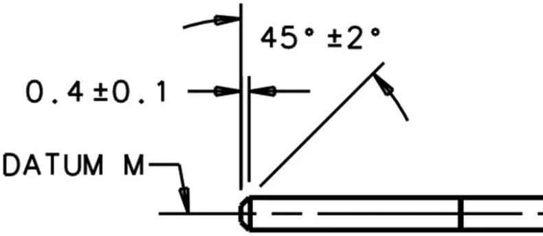
Commonly, it is 45°.
The angle range of the bevel is 20° to 45°. You can design the beveling angle according to the PCB thickness and the beveling depth below.
|
PCB copper thickness
|
Minimum pattern width/pattern interval
|
Minimum pattern width/pattern interval
|
Minimum pattern width/pattern interval
|
|
20°
|
1.6
|
0.5
|
1.51
|
|
2.0
|
0.65
|
1.85
|
|
|
2.5
|
0.7
|
2.47
|
|
|
30°
|
1.0
|
0.5
|
0.44
|
|
1.2
|
0.5
|
0.60
|
|
|
1.6
|
0.5
|
0.95
|
|
|
2.0
|
0.65
|
1.16
|
|
|
2.5
|
0.7
|
1.56
|
|
|
45°
|
1.0
|
0.5
|
0.25
|
|
1.2
|
0.5
|
0.35
|
|
|
1.6
|
0.5
|
0.55
|
|
|
2.0
|
0.65
|
0.68
|
|
|
2.5
|
0.7
|
0.9
|
Note: Why is there the remaining thickness? This is because all inner layers of the gold finger pad area need cutting copper during the PCB fabrication process. Both half-finger copper cutting and whole-finger copper cutting can be done by the PCB manufacturer.
Gold/nickel thicknesses of Edge Connectors
Edge connector pads are often applied with the surface finish of hard gold plating.
Hard gold plating includes two layers: a layer of gold alloyed with cobalt or nickel for hardness, and underneath it, the nickel layer between the alloyed gold and copper pads for prevention of the diffusion of gold into the copper.
The thicknesses of the gold and nickel layers of edge connectors are below:
- Au: 0.25um-1.5um
- Ni: ≥3um
Applications of Edge Connector Circuit Boards
Edge connectors are used for electrical connections between a PCB and another device or motherboard.
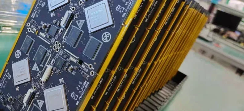
In a computer, you can find the expansion cards using edge connectors, such as the graphics card and sound card.
Circuit boards with edge connectors are used in far more applications including:
- Computer memory modules and expansion cards: graphics cards, memory sticks, sound cards, and network cards
- Industrial-grade storage and memory: Industrial storage modules, memory modules, embedded I/O modules, and industrial solid-state disks
- Embedded devices
- Transportation and network infrastructures
- Outdoor edge computing devices
- Servers
- Vehicle-mounted devices
One-Stop Edge Connector Circuit Board Manufacturing and Assembly
PCBONLINE is a source factory PCBA manufacturer, providing edge connector circuit board fabrication, component sourcing, PCB assembly, PCBA value-added, and box-build assembly.
Founded in 1999, PCBONLINE has two large advanced PCB manufacturing bases, one PCB assembly factory, stable supply chains for components and materials, and an R&D team.
Regarding the capabilities of edge connectors, PCBONLINE can make edge connectors with the thicknesses of Ni ≥3um and Au 0.25um-1.5um, minimum space between gold fingers of dry film pattern plating 0.175mm, and lead process 0.125mm.
Besides, the below surface finishes are available on the edge connector PCBs:
- ENIG +gold finger
- Flash gold(electroplated gold) + gold finger
- Immersion silver + gold finger
- Immersion Tin + gold finger
PCBONLINE provides free and professional DFM (design for manufacturing) for PCB/PCBA/box-build projects before and during the prototyping/sampling stage to ensure the success of your project and seamless mass production.
Strong manufacturing capabilities to meet your custom requirements for the edge connector PCB and PCBA, including the regular ones, uneven ones, and segmented ones.
One-stop PCBA manufacturing without hassles for you to integrate different manufacturers for different stages, including R&D, prototyping/sampling, PCB fabrication, component sourcing, PCB assembly, conformal coating, IC burn-in, comprehensive testing and inspections, enclosures, and box-build assembly for the final device.
High-quality edge connector circuit boards certified with ISO 9001:2015, ISO14001:2015, IATF 16969, RoHS, REACH, UL, and IPC-A-600 Class 2/3.
Free prototyping/sampling, R&D, PCBA functional testing, and IC burn-in for mass production orders.
With PCBONLINE as your PCBA partner, you can ensure the success of your project and save big in costs and time. For inquiries and quotes, contact PCBONLINE's team at info@pcbonline.com.
Conclusion
Edge connectors or PCB gold fingers are a row of hard gold-plated pads without components soldered. They are used for PCB insertion and contact with the alignment connectors of the motherboard. This blog delves into the specifications and details of circuit board edge connectors comprehensively. If you want to talk with experts in edge connector circuit boards, contact PCBONLINE by email or chat with us from the online chat window.
PCB assembly at PCBONLINE.pdf


