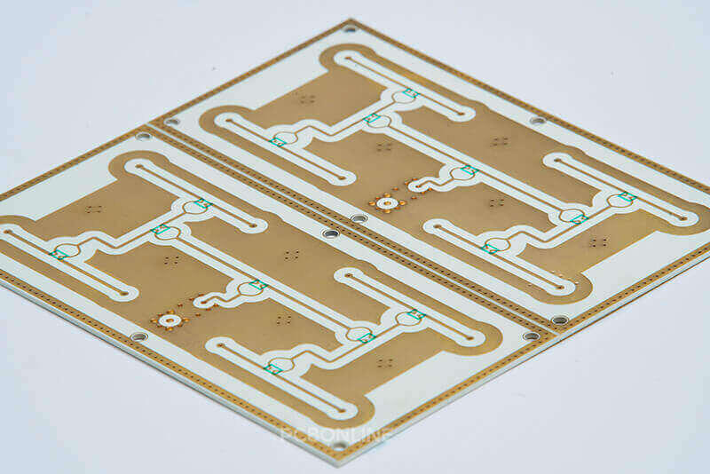
Printed Circuit Boards (PCBs) are the foundation of almost every electronic device, and they meet the demand for smart, small, and efficient electronics solutions. One major breakthrough in PCB design is the use of embedded components. In this blog, we'll explain PCB embedded components, why they're such a big deal, and dive into a real-world project to show how they make a difference.
In this article:
Part 1. What Are PCB Embedded Components? Part 2. PCB Embedded Components Real-World Project Part 3: One-stop PCBA Manufacturer for PCB with Embedded ComponentsWhat Are PCB Embedded Components?
Embedded components in PCBs are electronic parts like resistors, capacitors, or even integrated circuits (ICs) built right into the PCB instead of being placed on its surface. Unlike the more traditional surface-mounted or through-hole components, these parts are hidden within the layers of the PCB itself.
The types of PCB embedded components include:
- Passive components: Things like resistors, capacitors, and inductors.
- Active components: Includes diodes, transistors, and ICs.
- Special layers: Materials that manage heat or block electromagnetic interference (EMI).
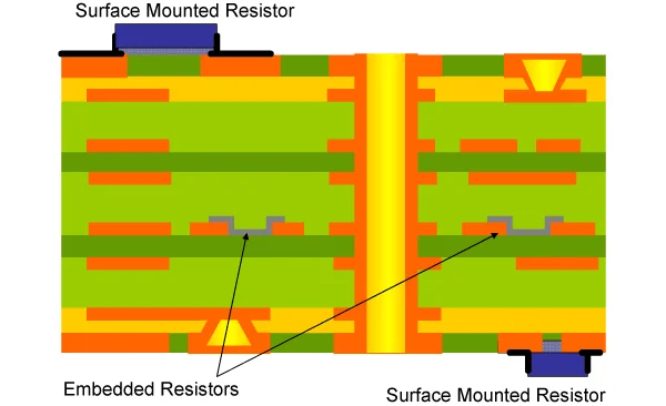
Figure 1: A cross-section of a PCB showing how resistors can be embedded right into the layers.
Why Use PCB Embedded Components?
Embedding components directly into the PCB has some awesome benefits:
- Smaller devices: By embedding components, you save a ton of space, which means smaller devices. This is a game-changer for wearables, IoT gadgets and smartphones.
- Better performance: Since embedded components are closer together, they have shorter electrical paths. This improves signal quality and reduces power loss.
- More durable: Components inside the PCB are protected from vibrations, shocks, and environmental stress, making them perfect for cars and airplanes.
- Cost savings: While it costs more upfront to design and manufacture, embedding components can save time and money in mass production by simplifying assembly.
6-layer PCBs can suffice a wide range of applications, including embedded systems, communication devices, IoT devices, RF systems, high-speed digital circuits, etc.
6-layer PCBs provide many benefits for a mid to high-end application project. Their benefits are as below.
- Signal integrity: Enhanced layer combination leads to reduced noise and crosstalk.
- Thermal management: Better heat dissipation.
- Compact design: Reduces size without compromising the complexity of the circuitry.
- Compliance with EMI/EMC: Enhanced shielding and isolation provide better EMI.
PCB Embedded Components Real-World Project: Compact Wearable Health Tracker
Take the wearable health tracker PCB as an example. This project showcases how embedded components can overcome challenges in designing compact, efficient, and durable devices.
Project overview: The project is to design a compact wearable health tracker capable of monitoring heart rate, body temperature, and physical activity while maintaining a sleek and lightweight design. The device had to be efficient, durable,e and wireless, making it perfect for daily use or fitness enthusiasts.
Key design challenges
1. Size constraints: The PCB had to fit into a casing measuring just 30mm x 30mm, leaving very little room for components.
2. Power efficiency: The device needed to run for several days on a small rechargeable battery.
3. Signal integrity: Accurate sensor data transmission to a smartphone app was essential.
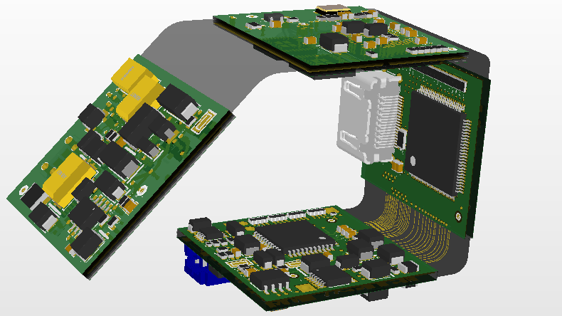
Figure 2: Early prototypes required significant downsizing to meet project goals.
Step-by-Step Approach to the Compact Wearable Health Tracker Project
Step 1: Define the project goals and requirements
The goal of this project is to design a compact, wearable health tracker capable of:
- Monitoring heart rate, body temperature, and physical activity.
- Maintaining a sleek, lightweight design suitable for daily wear and fitness activities.
- Ensuring power efficiency to operate for several days on a small rechargeable battery.
- Wirelessly transmitting sensor data to a smartphone app for real-time monitoring and analysis.
Step 2: Design the initial circuit and PCB layout
The first step was to design a functional prototype that met the project's size and performance requirements. Using Altium Designer, the following steps were taken:
(i)Component selection:
The selected sensors included a heart rate monitor, body temperature sensor, and accelerometer for physical activity tracking. A Bluetooth Low-Energy (BLE) module was chosen for wireless communication with the smartphone.
(ii)Power circuit design:
A compact Li-ion battery was selected to power the device, with a low-dropout regulator (LDO) for efficient voltage regulation. Passive components like resistors and capacitors were added for signal conditioning and stability.
Step 3: Switch to embedded components
To address the size constraints and improve power efficiency, the design was reworked to incorporate embedded components. Key steps included:
(i)Selection of embedded components:
Resistors, capacitors, and inductors were embedded within the inner layers of the PCB to save surface space and reduce component height. This allowed for a more compact design while maintaining performance.
(ii)Layer stack-up design:
The PCB was designed using a multi-layer configuration to maximize available space.
The top and bottom layers were used for active components like the sensors and Bluetooth module.
Inner layers were used for embedded passive components and power planes.
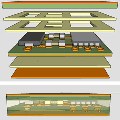
Figure 3: Multilayer PCB design showing the embedded components and their placement within the inner layers of the PCB.
(iii)Thermal management:
Thermal vias were incorporated around critical components to ensure proper heat dissipation, maintaining component longevity and performance.
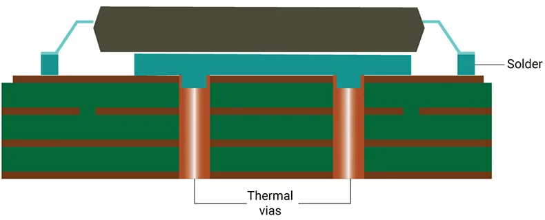
Figure 4: Illustration of thermal vias used in the PCB design to manage heat dissipation for embedded components.
Step 4: Optimize power efficiency
Since the device needed to run for several days on a small battery, power efficiency was a top priority. Key steps taken included:
(i)Custom power circuit design:
The embedded power management components helped reduce voltage ripple and optimize battery charging and discharging cycles, ensuring efficient energy use.
(ii)Power plane design:
A dedicated power plane was added to the PCB to ensure an even and efficient distribution of power to the sensors and wireless module. This minimized power loss and maximized battery life.
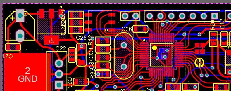
Figure 5: Power circuit design with embedded power management components
Step 6: Finalize and manufacture
(i)Compact enclosure design:
The PCB's reduced size allowed it to fit into a slim, comfortable wearable case. The final design was lightweight, durable, and comfortable enough to be worn daily.
(ii)Scalability considerations:
The embedded components simplified assembly, reduced the overall footprint, and streamlined production, cutting both time and cost.
Figure 6: Wearable health tracker prototype showcasing its sleek and compact design.
Benefits of PCB Embedded Components in This Project
Space savings: Embedding passive components allowed for a 35% reduction in PCB surface area, enabling a compact and wearable device.
Improved performance: Shorter signal paths and optimized component placement minimized power loss and enhanced the reliability of wireless transmission to the smartphone app.
Power efficiency: The custom embedded power circuit ensured extended battery life, allowing the device to function for several days without frequent charging.
Durability: Embedded components were shielded from environmental factors, such as moisture and temperature extremes, ensuring the device remained functional under various conditions.
One-stop Embedded Component PCB Manufacturer PCBONLINE
If you need R&D, prototyping, PCB manufacturing, PCB assembly, comprehensive testing, and value-added services for embedded component PCB projects, you can work with PCBONLINE, a one-stop advanced PCB manufacturer.

Founded in 1999, PCBONLINE has two large advanced PCB manufacturing bases, one PCB assembly factory, stable supply chains, and an R&D team.
PCBONLINE provides turnkey electronics manufacturing services for embedded-component PCB projects, including software and hardware R&D, PCB prototyping, PCB manufacturing, component sourcing, PCB assembly, PCBA functional testing, thermal aging, IC programming, enclosures, and box-build assembly.
PCBONLINE offers free one-on-one engineering support and DFM for embedded-component PCB projects, ensuring the smooth manufacturing process and successful results of the boards and end-devices.
Various embedded-component PCBs custom meet your project demands, such as FR4 PCBs, rigid-flex PCBs, Rogers high-frequency PCBs, HDI PCBs, and ceramic PCBs.
High-quality embedded-component PCB manufacturing certified with ISO 9001:2015, ISO 14001:2015, IATF 16949:2016, RoHS, REACH, UL, IPC-A-600 Class 2/3, and IPC-A-600 Class 2/3.
When your embedded-component PCB project enters the bulky production stage, PCBONLINE refunds the fees for R&D, prototyping/sampling, and PCBA functional testing.
Besides embedded-component PCBs, PCBs can embed copper busbars and ceramic PCB inlays in the PCB. To get a quote, please contact info@pcbonline.com.
Conclusion
By utilizing embedded components, a PCB achieves optimized power efficiency, reliable signal transmission, and a sleek, lightweight form, ideal for compact devices. If you're ready to explore the possibilities of embedded components and compact PCB designs, PCBONLINE is ready to assist.
PCB fabrication at PCBONLINE.pdf


