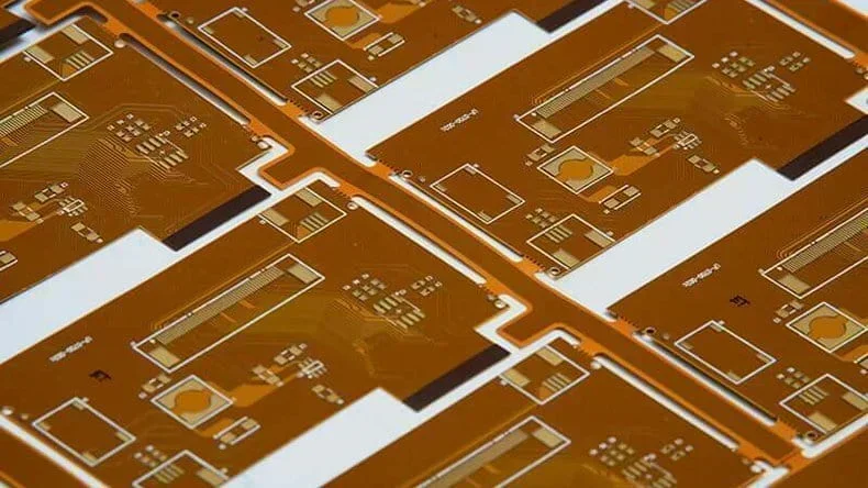
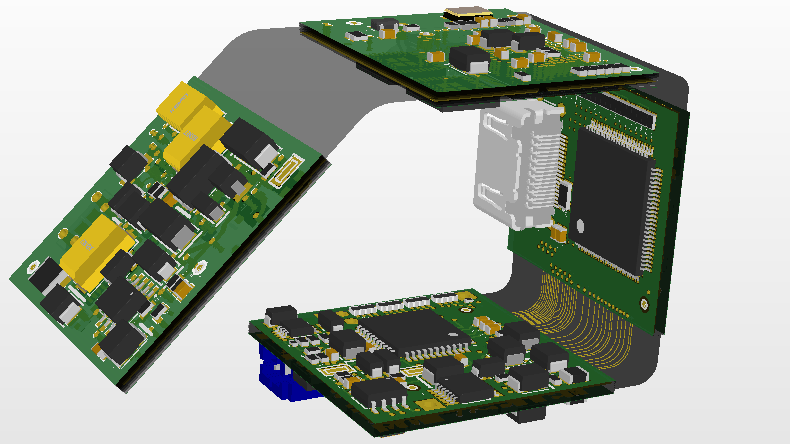
Flexible PCBs are circuit boards built on polyimide (PI) or polyester (PET) substrates. They are lightweight and can bend, twist, or flex while maintaining electrical performance. Flexible PCBs offer 3D design freedom, space efficiency, and flexibility, making them the backbone of wearable devices, foldable display screens, compact medical devices, robotics, etc.
What does it take to design a reliable flexible PCB? Let's examine a real-world project and explore some design tips to explore the process.
In this article:
Part 1. How to Design Flexible PCB: A Smart Fitness Band Part 2. Key Considerations in Flexible PCB Design Part 3. Tips for a Successful Flexible PCB Design Part 4. Challenges and Trends for Medical PCBs Part 5. Challenges in Flexible PCB Design One-stop Flexible PCB Manufacturer with R&D CapabilitiesHow to Design Flexible PCB: A Smart Fitness Band
This article uses a project example of designing a flexible PCB for a smart fitness band. The challenge is to fit key components like a heart rate sensor, accelerometer, Bluetooth module, and rechargeable battery into a sleek and curved design. The project's aim is to ensure the PCB can handle the bending and twisting while maintaining functionality.
Step 1: Define the design objectives
The fitness band needs to integrate several key components:
- Heart rate sensor: For pulse monitoring.
- Accelerometer: To track movement and activity.
- Bluetooth module: For wireless communication.
- Rechargeable battery: Providing power to the system.
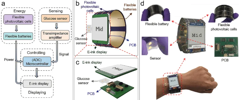
The PCB size was defined at 40mm x 10mm, to fit within the slim and curved housing of the band. A 4-layer stackup was chosen for better signal integrity, power distribution, and ground isolation, which is essential for wireless communication and sensor accuracy.
Fit all components into the specified form factor.
Ensure durability under daily bending and twisting.
Step 2: Material selection
To support the band's dynamic movements, I selected a polyimide substrate. The PI material offers the flexibility and thermal stability necessary for the design. Adhesives and PI protective films were also chosen to enhance durability while maintaining the flex PCB's lightweight nature.

Step 3: Create the schematic design
Using Altium Designer, I developed the schematic to interconnect all components. Key considerations included:
- Proper power routing to minimize noise.
- Ensuring clean signal paths for the Bluetooth module.
- Incorporating over-current protection for the battery circuit.
This stage required careful planning to ensure a compact layout without sacrificing performance.
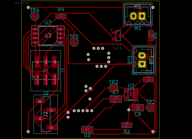
Step 4: Flexible PCB layout
The layer stackup of the four-layer flexible PCB consists of:
- Top layer: Primary signal routing for the components.
- Inner layer 1: Ground plane, providing better grounding and reducing noise.
- Inner layer 2: Power plane, ensuring stable voltage to sensitive components.
- Bottom layer: Additional signal routing.
Key design considerations in the PCB layout in a 4-layer flex PCB design:
Component placement: Components are placed strategically on flat areas of the PCB to minimize mechanical stress.
Trace routing: To minimize stress during bending, I used rounded corners and kept traces perpendicular to the bending axis.
Ground and power planes: The inner layers dedicated to ground and power planes ensure stable operation and reduced signal noise.
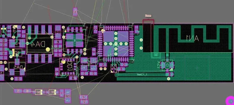
Step 5: Simulations and analysis
Before prototyping, several simulations should be conducted to validate the design:
- Signal integrity analysis: Ensure reliable ECG and Bluetooth data transmission.
- Mechanical simulations: Verify the PCB's resilience under repeated bending and twisting.
- Thermal analysis: Check for adequate heat dissipation, particularly around the Bluetooth module and battery.
Step 6: Flexible PCB prototyping and testing
Send the Gerber of the flexible PCB to the one-stop advanced PCB manufacturer PCBONLINE. PCBONLINE provides one-on-one engineering support and free design for manufacturing (DFM) to ensure the success of the flexible PCB project. After PCB prototyping, PCBONLINE has comprehensive testing and inspection of the flexible PCB prototype, including but not limited to:
Dynamic bending tests were conducted with a setup that simulated real-world use. The PCB has bent over 100,000 cycles, exceeding the expected lifetime of the product.
Functional tests ensured the sensors, Bluetooth communication, and battery charging worked flawlessly.
After testing, there may be iteration and refinement. Based on testing feedback, minor adjustments are made to improve durability and optimize signal performance. The final design will be sent for mass production also at PCBONLINE after successful testing.
Key Considerations in Flexible PCB Design
1. Material mattersChoosing the right material is crucial. Polyimide is a common choice due to its flexibility and high-temperature resistance. For applications requiring transparency, polyester is used, but it's less durable under high temperatures.
2. Define the bend radiusThe bend radius is the minimum radius a PCB can flex without damaging the copper traces or substrate. A good rule of thumb is to keep the bend radius at least 10 times the thickness of the PCB.
3. Component placementAvoid placing components or vias in areas prone to flexing. Use rigid-flex designs if components need to be placed on both flexible and rigid areas.
4. Trace routingUse rounded corners: Avoid sharp 90-degree angles in trace routing to minimize stress.
Use hatched ground planes: Solid planes can lead to cracking during flexing. Hatched planes offer better flexibility.
Keep traces perpendicular to the bend: This reduces stress and improves durability.
Tips for a Successful Flexible PCB Design
Flex PCBs require different manufacturing processes compared to rigid PCBs. Engage with your manufacturer during the design phase to ensure your flex PCB design is manufacturable. For example, some manufacturers may have limitations on minimum trace widths or bend radius.
2. Use DFM toolsDesign for Manufacturability (DFM) tools can help you identify potential issues before sending your design for fabrication. This step can save time and reduce costly redesigns.
3. Protective coatingsApply coverlays or protective films over the flexible PCB to safeguard against environmental factors like moisture, dust, or physical wear.
4. Keep thermal management in mindFlexible PCBs in high-power applications can overheat due to limited heat dissipation. Use thermal vias and adequate spacing to manage heat effectively.
5. Consider stiffenersIf your design involves connectors or soldered components, use flex PCB stiffeners to provide mechanical support and prevent stress on the flexible substrate.
Challenges in Flexible PCB Design
1. CostFlexible PCBs are often more expensive than rigid ones. However, the cost can be offset by their ability to replace multiple rigid PCBs and connectors.
2. Manufacturing tolerancesMaintaining tight tolerances during manufacturing is challenging. Ensure your design considers the manufacturer's capabilities.
3. Reliability in dynamic environmentsEnsuring long-term reliability under constant bending or twisting requires rigorous testing and careful design.
Designing a flexible PCB may seem challenging but it's a highly rewarding process that unlocks endless possibilities for innovative electronics. Success depends on thoughtful planning and execution from choosing materials that can handle bending and movement to optimizing component placement and trace routing. Testing for durability, heat resistance and signal quality ensures the design performs reliably in real-world conditions.
One-stop Flexible PCB Manufacturer with R&D Capabilities
If you're ready to bring your flexible PCB ideas to life, the one-stop flexible PCB manufacturer PCBONLINE is ready to help. Founded in 1999, PCBONLINE has two large advanced PCB manufacturing bases, one PCB assembly factory, stable supply chains, and an R&D team.

PCBONLINE has turnkey flexible PCB manufacturing capabilities. It not only fabricates and assembles flexible PCBs, but also provides flexible copper-clad laminates custom for flexible PCB fabrication.
PCBONLINE has flex project R&D capabilities and can do the flexible PCB design or take part in your project's development from the early stage.
Strong flexible manufacturing capabilities, including transparent PET flexible PCBs and 1 to 8-layer PI flexible PCBs with a maximum length of 200m.
PCBONLINE provides free design for manufacturing (DFM) and one-on-one engineering support for flexible PCB and PCBA projects.
High-quality flexible PCBs certified with ISO 9001:2015, ISO 14001:2015, IATF 16949:2016, RoHS, REACH, UL, and IPC-A-610 Class 2/3.
The professional team at PCBONLINE specializes in creating high-quality flexible PCBs tailored to your project's custom needs. To get a quote for your flexible PCBs, please contact info@pcbonline.com.
Conclusion
This blog takes the wearable fitness band PCB for example to illustrate how to design flexible PCBs. This project highlights how flexible PCBs enable compact, cutting-edge devices. With careful design choices and the right materials, the flex PCB combines functionality and durability, remaining dependable even with frequent bending or exposure to different environments. To design and manufacture flexible PCBs for your application project, work with PCBONLINE.
PCB fabrication at PCBONLINE.pdf


