
As the Internet of Things (IoT) technology develops, the demands for High-Density Interconnect (HDI) PCBs increase because electronic devices are getting smaller, smarter, and more multifunctional. HDI PCBs are the backbone of IoT devices, from smart home gadgets to industrial controllers. How to design HDI PCBs for IoT devices? This blog uses an HDI PCB design project example for smart door locks to reveal IoT HDI PCB design step by step.
In this article:
Part 1. What is HDI PCB for IoT Devices? Part 2. IoT HDI PCB Design Example: Designing an HDI PCB for a Smart Door Lock Part 3. One-stop HDI PCB Manufacturer for IoT ProjectsWhat is HDI PCB for IoT Devices?
Characterized by their high density of interconnections, HDI PCBs can accommodate more components in smaller spaces. HDI PCBs are designed with finer lines and spaces, smaller vias, and higher component densities compared to normal FR4 multilayer PCBs.
HDI PCBs features:
- Microvias: Small-diameter vias that connect different PCB layers.
- Blind and buried vias: Vias that either start or end within internal layers, saving space on the surface.
- Thin substrates: Enables compact designs while maintaining structural integrity.
- High signal integrity: Reduced electromagnetic interference (EMI) and improved signal performance.
IoT devices demand compactness, efficiency, and high functionality. HDI technology addresses all the IoT requirements:
Miniaturization: Devices like smartwatches and medical wearables benefit from HDI's microvias and compact designs, enabling small footprints without sacrificing features.
High-speed connectivity: IoT devices rely on fast data transfer. HDI PCBs ensure reliable signal integrity, crucial for communication modules.
Component density: IoT devices integrate multiple components like sensors and microcontrollers. HDI's dense layouts accommodate these without increasing size.
Power optimization: Battery-powered IoT devices benefit from shorter trace lengths and efficient routing, reducing power consumption.
IoT HDI PCB Design Example: Designing an HDI PCB for a Smart Door Lock
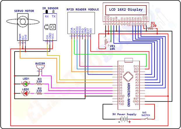
A smart door lock integrates a fingerprint scanner, Bluetooth module, and a motorized locking mechanism. Let's dive into how you can design an HDI PCB for smart door locks in Altium Designer.
Step 1: Define requirements
Before starting the design, define the following:
- 1. PCB size: Slim enough to fit inside a door lock housing.
- 2. Key components: Microcontroller, Bluetooth module, motor driver, battery management system, and fingerprint sensor.
- 3. Layer stack-up: At least 6 layers for signal routing, power distribution, and ground planes.
Step 2: Set up the project in Altium Designer
Start a new project:
- Open Altium Designer and create a new PCB project.
- Define the board size ( 50mm x 30mm for a compact door lock).
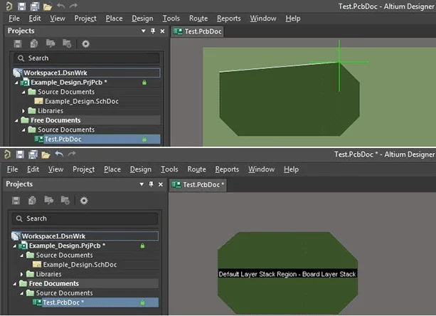
Initial board size setup for the smart door lock PCB in Altium Designer
Define the layer stack-up:
- Open the Layer Stack Manager.
- Configure a 6-layer stack with the following:
- Top Layer: Component placement and high-speed signals.
- Internal Layers: Power, ground, and signal layers.
- Bottom Layer: Secondary components and traces.
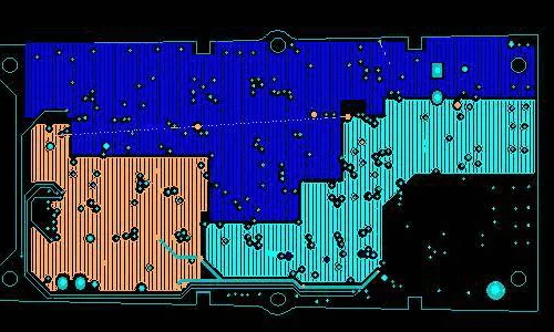
Layer stack configuration for a 6-layer HDI PCB in Altium Designer
Step 3: Schematic design
Place components:
- Add components like a microcontroller, Bluetooth module, and motor driver.
- Use the Altium libraries or import parts from manufacturers' databases.
Connect components:
- Draw connections for data, power, and control signals.
- Optimize placement to reduce trace lengths.
Schematic of the smart door lock showing key components and connections
Step 4: PCB layout design
The PCB layout stage is critical for translating the schematic into a functional physical design. For the smart door lock, component placement plays a pivotal role. Components such as the microcontroller, Bluetooth module, and motor driver must be arranged to minimize trace lengths and prevent interference. For instance, the Bluetooth antenna should be positioned away from noisy components like the motor driver to maintain signal quality.
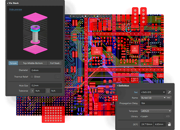
Routing is another essential aspect. HDI PCBs utilize microvias, blind vias, and buried vias to create interconnections between layers without taking up valuable surface space. For the smart door lock, PCB microvias are employed to connect the densely packed components across the six-layer stack-up. High-speed signal traces are carefully routed with impedance control to ensure reliable communication between the microcontroller and Bluetooth module. Additionally, dedicated power and ground planes in the internal layers help reduce electromagnetic interference and improve overall circuit stability.
Thermal management is also considered during the layout phase. Thermal vias are added near heat-generating components like the motor driver to dissipate heat efficiently. These design considerations ensure the PCB remains reliable under continuous operation, even in compact housings like a smart door lock.
Step 5: Validation and Preparation for PCB Manufacturing
Final HDI PCB design for the smart door lock
After completing the layout, validating the PCB design is crucial to avoid potential issues during manufacturing or operation. Design Rule Checks (DRC) are performed to ensure all traces, clearances, and vias meet the specified constraints for HDI PCB fabrication. For example, DRC can identify violations in trace widths or spacing, which are critical for the dense routing typical in smart door locks.
Signal integrity analysis is another important step, especially for high-speed communication lines. Altium Designer's simulation tools are used to evaluate and refine the impedance of critical traces, ensuring reliable performance. For the smart door lock, this step is essential for maintaining stable communication between the Bluetooth module and microcontroller.
Once the design is validated, the final step involves exporting manufacturing files. Gerber files, drill files, and the Bill of Materials (BOM) are generated and shared with the manufacturer. These files contain all the necessary information for fabrication and assembly, ensuring the design is accurately replicated. Additionally, detailed assembly drawings are prepared to guide the placement of components, especially critical ones like the fingerprint sensor and Bluetooth antenna.
One-stop HDI PCB Manufacturer for IoT Projects
If you're ready to explore the possibilities of HDI PCBs for IoT devices, the one-stop HDI PCB manufacturer PCBONLINE is ready to help.
PCBONLINE provides 4-to-64-layer HDI PCB fabrication, assembly, and PCBA box-build assembly for IoT applications. HDI PCBs can be manufactured in various substrate materials and types, such as FR4, polyimide (flexible PCB), polyimide + FR4 (rigid-flex PCB), and PTFE/Rogers (high-frequency PCB).

3000m² of production capacity per day for HDI PCBs with builds of 1+N+1, 2+N+2, 3+N+3,4+N+4, and arbitrary interconnection in any layers.
PCBONLINE has hardware and software R&D capabilities for IoT applications, including PCB design and enclosures.
We can manufacture complex HDI PCBs for IoT devices, inlay boards, heavy copper designs, and hybrid and fine structure lay-ups.
Besides HDI PCB fabrication, we have powerful capabilities in fine-pitch assembly for HDI PCB assembly.
We have rich R&D and manufacturing experience for HDI PCB applications such as FPGA boards. High-quality HDI PCB and PCBA manufacturing certified with ISO 9001:2015, IATF 16949, RoHS, REACH, UL, and IPC-A-610 Class 2/3.
If you need HDI PCBs or technical support for your IoT device project, please send your email to PCBONLINE at info@pcbonline.com. We will provide one-on-one engineering support to you.
Conclusion
This blog takes the smart door lock PCB as an example to showcase how HDI PCB design techniques can overcome challenges in creating compact, efficient, and durable IoT devices. HDI PCB design achieves optimized power efficiency, reliable signal transmission, and a sleek, lightweight form ideal for modern smart home applications. If you need one-stop electronics manufacturing for your IoT project, contact the HDI PCB manufacturer PCBONLINE for high-quality IoT PCB solutions tailored to your project's needs.
PCB assembly at PCBONLINE.pdf


