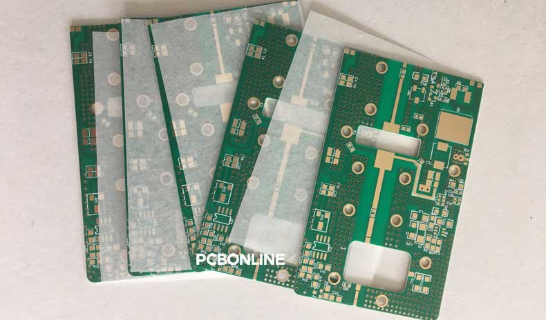
Designing PCBs for high-speed functions is a greater challenge. Designers can make it in high-speed PCB design through governed layer stack-up, controlled impedance routing, and qualitative positioning of parts. This is exemplified by the 6-layer communication module which implements these concepts and thus serves well in networking and embedded systems operation.
The common challenges in high-speed PCB design include cross-talk, signal reflection, and EMI issues.
Crosstalk: Signaling interference originates from one or more neighboring traces.
Solution: Insert different level planes for routing forward and return pathways of high-speed signals, as well as increase the distance between traces.
Signal reflection: Signals get distorted as a result of the existence of impedance discontinuities.
Solution: Employ controlled impedance traces and provision of cynosure termination resistors.
EMI issues: The emission of electromagnetic energy results from the propagation of signals at a high speed, which causes interference with other parts.
Solution: Mitigate trace length and guide signals through solid ground planes.
To solve the challenges, the key considerations in high-speed PCB design include layer stack-up design, impedance control, ground and power integrity, component placement, and signal routing. The below content and images use the same 6-layer high-speed PCB to reveal these considerations in high-speed PCB design one by one.
In this article:
1. Layer Stack-Up Design 2. Impedance Control 3: Ground and Power Integrity 4. Component Placement 5. Signal Routing One-stop High-speed and High-frequency PCB Manufacturer1. Layer Stack-Up Design
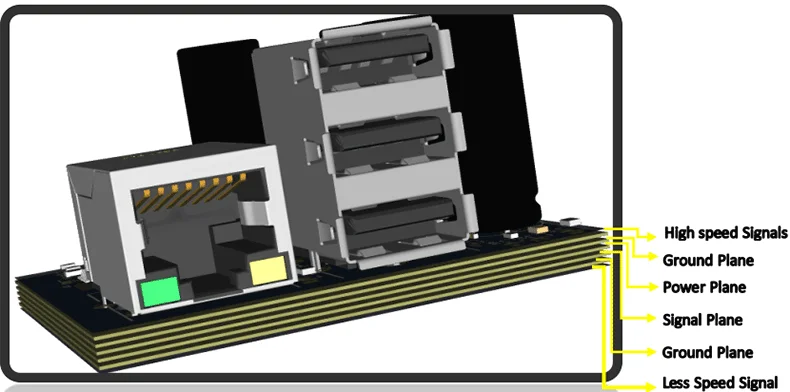
The sequence of conductive and dielectric layers in PCB is a layer stack-up configuration. It is important for ensuring reliable power distribution, electromagnetic interference suppression, and signal transmission. For high-frequency PCBs, an appropriate stack-up design will limit cross-talk, provide consistent reference planes, and ease the handling of impedance. The 6-layer stack-up for the example communication module PCB is:
- Top layer: High-speed signal traces (Ethernet, USB cables)
- Layer 2: Ground plane
- Layer 3: Power plane (3.3V, 1.8V supply)
- Layer 4: Another signal-routing layer
- Layer 5: Additional ground plane
- Bottom layer: Connectors and signals of lesser speeds
In the 6-layer communication PCB example, Ethernet traces, and USB differential pairs are run on the first layer of the communication module while their return paths run above the second layer ground patch.
2. Impedance Control
Impedance matching tends to maintain the integrity of the signal without distortions and reflections. When densities are larger with high-speed transmission, differential pairs of Ethernet and USB for instance will need specific impedances. To achieve 90Ω (USB) or 100Ω (Ethernet), the following materials are used to create differential pairs of Tx+/Rx-:
- Controlled trace widths and separation.
- During simulations, an integrated approach for maintaining impedance consistency along the entire signal pathway should be verified.
The best person to contact for assistance on how to select the correct dielectric material and stack-up properties is your PCB manufacturer. The high-speed and high-frequency PCB manufacturer PCBONLINE offers one-on-one engineering support throughout your project, no worries about your high-speed PCB design by working with PCBONLINE.
3. Ground and Power Integrity
In high-speed PCBs, power and ground structures are important for reliable operation. The power distribution planes maintain the required voltage levels and the ground planes provide low impedance for the return of the signals. Here is how to achieve this:
- Employ partitioned layers for ground and power.
- High enough loop inductance should be made low enough and connection between ground layers accomplished by means of stitching "vias".
- To absorb stray power, place the decoupling capacitors as near as feasible to the power of the IC pins.
In the 6-layer communication PCB example, a case in point is when the communication module has stitching vias at places of high current and places Layer 2 and Layer 5 for ground and Layer 3 for power (3.3V and 1.8V).
4. Component Placement
The first stage of PCB design is component placement, which enables signal integrity to be maintained and routing less complex. Proper placement directly impacts the performance and reliability of high-speed PCBs.
- Shortest signal paths: The Ethernet PHY, for example, should be placed next to connectors like RJ45, which will aid in minimizing the trace lengths.
- Clock source positioning: In order to reduce jitter, it is recommended that oscillators be located closely to the integrated circuits they service.
- Accessibility: On the edges of the PCB, RJ45 and USB-C connectors are to be placed.
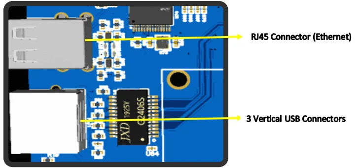
In the 6-layer example PCB design, to facilitate proper routing, the communication module integrates the Ethernet PHY with the RJ45 connector and the USB 3.x controller with the USB-C connector.
Best Practices
- Grouping related components: Place decoupling capacitors close to IC power pins.
- Avoid overcrowding: Create sufficient clearance to enable heat to be dissipated as well as traces to be routed.
- Thermal considerations: For better cooling, place the elements that radiate heat like SoC to the nearby copper pours.
5. Signal Routing
Signal routing defines the physical routes that voltage or current can follow between different components on the PCB. This is among the critical steps in high-speed PCB design, as the routing decisions influence the performance of the device. Below are what to know about signal routing for high-speed signals, clock signals, and power and ground.
High-Speed Signal routing
The performance level is influenced by the interconnection of the high-speed signals which is a sensitive task. Differential pair routing and Trace geometry must be properly done. Some restrictions accompany the routing of high-speed signals in the PCB design:
Differential pair routing:To ensure the signal reaches its destination in the correct order, match the trace lengths.
Maintain signal integrity with the help of symmetrical vias.
Trace geometry:To reduce signal reflection, 90-degree bends should be avoided, while 45-degree bends can be used.
To minimize electromagnetic interference (EMI), communication should be routed over surfaces with uninterrupted ground planes.
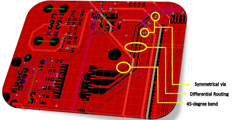
In the communication module PCB example, the Ethernet differential pairs in the communication module are routed using length-matched traces between the PHY and RJ45 with a 100Ω impedance.
Clock Signal routing
The clock signals need to be routed carefully as they are very loud in their reception and can become inaccurate, therefore the following needs to be observed:
- The clock traces should be kept as short and straight as possible to reduce unwillingness and delay.
- It should be routed over a firm ground plane.
- Termination resistors should be used to minimize reflection.
Power and Ground Routing
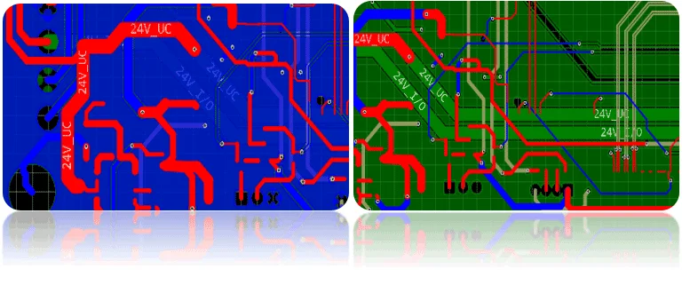
Routing power and ground involves maintaining a stable power delivery network (PDN) and ensuring minimal noise.
- Power planes: For every level of voltage (for instance 24 volts, 3.3 volts, or 1.8 volts) there should be a designated region.
- Ground planes: Every time other ground planes are used, there is a reduction in EMI interference and another reference is introduced.
- Decoupling: For optimal results, the decoupling capacitors should be situated as closely as possible to the power pins.
Validation and Simulation
After the signal routing, the high-speed PCB design still needs validation and simulation.
Signal integrity analysisHigh-speed signals are guaranteed to retain their intended properties throughout the PCB thanks to signal integrity analysis.
- Create differential pair impedance models and crosstalk models with the help of various programs such as Ansys HFSS, and Cadence Sigrity.
- For data communication check upon skew and trace lengths to ensure transmission is smooth.
Power integrity analysis identifies voltage ripple and noise issues that can impact circuit performance.
- To check ripple and maximum noise assessment employ SPICE-based simulation tools.
- Ensure that power is transferred with minimal fluctuations and noise ensuring that it operates around a stable point.
Prototyping and Testing
- Develop rough drafts or prototypes and compare them using high-speed oscillators confirming if it is working as intended.
- Look out for how devices such as USB and Ethernet work in terms of how fast they process data.
In the high-speed PCB example, the performance of an Ethernet communication module prototype can be measured using USB compliance testing tools and packet generators.
One-stop High-speed and High-frequency PCB Manufacturer
If you have a project plan for high-speed or high-frequency applications, whether you have completed the high-speed PCB design or not, you can work with the one-stop advanced PCB manufacturer PCBONLINE for R&D and turnkey PCB manufacturing.

Founded in 1999, PCBONLINE has two large advanced PCB manufacturing bases, one PCB assembly factory, stable supply chains, and an R&D team.
Provide one-stop high-speed and high-frequency PCB manufacturing, including R&D, prototyping, PCB fabrication, component sourcing, PCB assembly, PCBA value-added, and box-build assembly.
Minimum laser drill: 0.075mm, minimum mechanical drill: 0.15mm, with microvia structures of 100 µm and 125 µm. High-density circuit layers up to 20, and microvia layers up to 64.
PCBONLINE grasps the core technologies for high-speed PCB manufacturing, such as impedance control, embedded antenna DFM, expansion/contraction control, etc.
Have ready-to-use high-speed PCB base materials in stock, and the storage period is within 45 days (at manufacturers who have no storage, it usually takes 2 to 3 months to purchase base materials).
High-quality high-speed and high-frequency PCB manufacturing certified with ISO 9001:2015, ISO 14001:2015, IATF 16949:2016, RoHS, REACH, UL, and IPC-A-600 Class 2/3.
PCBONLINE pays attention to quality and cost-effectiveness in high-speed PCBs. If you want to get a quote or ask questions, you can send emails to info@pcbonline.com to get a quote.
Conclusion
All stages of a high-speed PCB design ought to be thoroughly taken care of and executed. In this blog, the 6-layer communication module realizes the high-speed PCB design concepts in networking and embedded systems. If you need high-speed PCBs or PCBA, work with the one-stop PCBA manufacturer PCBONLINE.
PCB fabrication at PCBONLINE.pdf


