In the realm of printed circuit boards, the most complex and advanced PCBs are IC test boards and high-frequency backboards. The one-stop advanced PCB manufacturer and assembler PCBONLINE provides these complex circuit boards from prototypes to bulky production.
IC test boards include probe cards, load boards, and burn-in boards (BIB). In this article, you will learn about these semiconductor test boards one by one.
What are IC Test Boards?
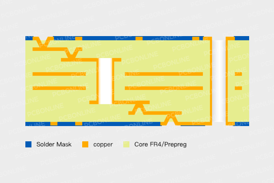
Semiconductor test boards or IC test boards, are also called IC carrier boards or IC substrates. They are considered the most high-end PCBs. The main function of IC test boards is to carry the IC as a carrier and connect the signal between the chip and its internal circuit.
Rigid PCBs have undergone a series of innovations from multilayer PCBs, traditional HDI PCBs, and SLP (substrate-like board) to IC test boards. SLP is a rigid printed circuit board similar to the IC carrier technology.
From the perspective of the production area, in 2018, China's IC carrier board companies accounted for 5% of the global market. Japanese companies accounted for about 23%, mainly distributed in the high-end carrier board market. Taiwanese companies accounted for about 37%. The rest are Korean, European, and American companies. In recent years, the market ratio of Chinese companies has gotten higher.
From the perspective of product type, semiconductor test boards are divided into the following three types of PCBs: probe cards, load boards, and burn-in boards (BIB).
Before the detailed introduction to these three types of IC test boards, here's a brief overview of them for your straightforward understanding.
|
Probe card
|
Load board
|
Burn-in board
|
|
|
Function
|
Wafer-grade electrical testing
|
IC package electrical testing
|
Thermal aging in high temperatures and high-pressure
|
|
Is used in which IC test
|
Wafer test
|
Final test after packaging
|
Reliability test
|
|
PCB features
|
HDI structure with ultra-fine traces. Its high-density probe contacts the wafer.
|
It connects the ATE (automated test equipment) to conduct the chip functional test. It has high requirements for high-speed signal integrity.
|
It should be able to work in high temperatures in the long term. It carries a large number of chips and tests them.
|
One-by-One Introduction to Probe Card, Load Board, and BIB
The probe card, load board, and burn-in board are the three main types of semiconductor test boards. They serve different functions in IC testing.
Probe Card
In a chip probing (CP) test, a probe card is used to connect the tester and the Pad on the Die, as the physical interface of the load board.
A probe card is attached to the load board through sockets or other interface circuits.
The probe card signal is converted by the interposer intermediary layer so that the probe of the probe head can receive the signal, and the signal can also be transmitted to the test machine for interpretation.
Application: Before the wafer is cut, the wafer quality can be tested by the probe card to avoid packaging costs caused by bad products.
Load Board
A load board is a mechanical and circuit interface connecting the test equipment and the device under the ATE.
It's mainly used in the yield test after IC packaging in the back end of semiconductor manufacturing/packaging.
Through the yield/final test, ICs with poor functions can be eliminated, and subsequent electronic products can be avoided due to defective ICs.
According to different test platforms, the IC test load board is divided into 93K series, T2000 series, TUF series, etc.
BIB (Burn-in Board or Aging Test Board)
ICs that have completed the final test after packaging are tested for burn-in under specific conditions and time to verify the reliability of the IC.
In thermal aging, the BIB carrying the chips is usually placed in a burn-in chamber at high temperatures above 125°C.
Through the aging test, early failure screening is prevented to ensure the chips are reliable in harsh environments.
As BIBs works in high temperatures, they are multilayer high-Tg PCBs.
One-stop IC Test Board Manufacturer PCBONLINE
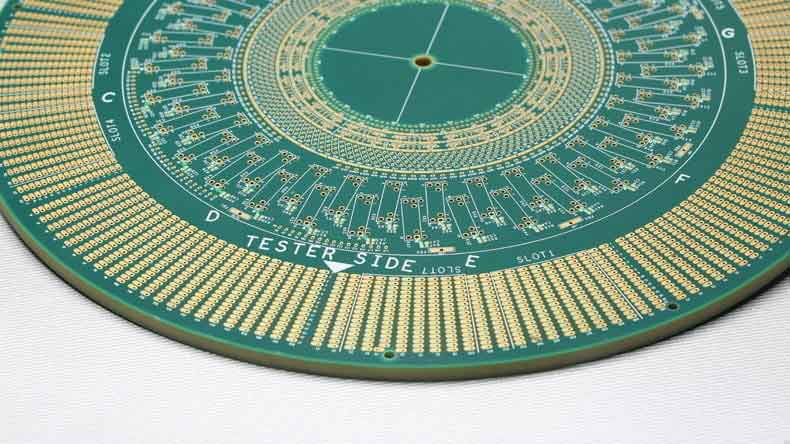
In this article, we share a load board production case by the manufacturer PCBONLINE.PCBONLINE is an advanced PCB manufacturer and assembler founded in 1999. It has two large advanced PCB manufacturing bases, one PCB assembly factory, stable supply chains, and an R&D team.
Layers: 38L
Thickness: 6.35mm
Material: TU872SLK
Aspect ratio: 30:1. Resin plug holes, electroplated and filled
Surface Treatment: Full board 30U” + partial OSP
Special: PTH spigot
Size: 768mm*570mm
DUT: 0.2mm
PIN-LAM: Multi-layer high-speed FPGA
PTH: High thickness ratio diameter copper filling technology
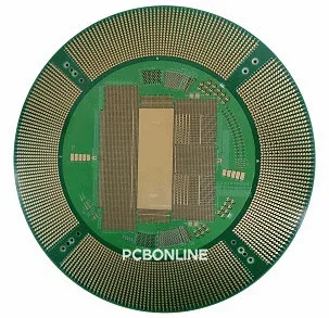
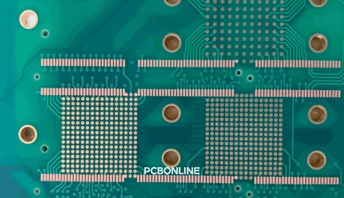
Below are some details about this load board shown in the below pictures.
Detail 1: PTH countersunk hole
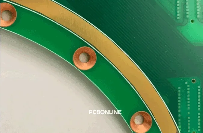
Detail 2: Hard gold + partial OSP
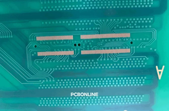
Detail 3: Selective hard gold 30U”
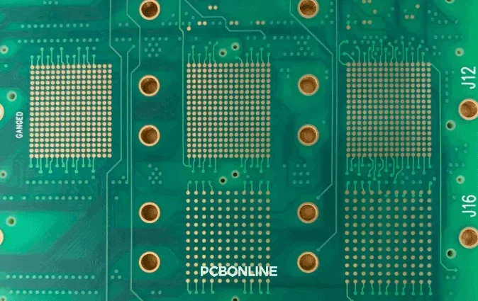
Detail 4: Selective hard gold 30U"+OSP
Are there challenges in the production process? Yes.
As ICs are becoming more sophisticated, more and more functions need to be tested, the number of layers of the UC test boards is getting larger, and the size is getting smaller.
Therefore, the following four aspects need to be strictly controlled:
1. Lamination deviation
2. Ultra-high thickness to diameter radio
3. Lager size resin plug hole
4. A variety of selective surface methods
We solved the challenges and provided the probe cards of the best quality to our client.
PCBONLINE's load board and probe card capabilities are below.
Load board/probe card |
Normal capabilities
|
Advanced capabilities
|
Limit capabilities
|
|
PCB size (inches)
|
≤18*24
|
20*24
|
21*25
|
|
Min DUT pitch (mm)
|
≥0.65
|
0.5-0.4
|
0.35
|
|
Layer
|
≤28
|
30 to 52
|
52+
|
|
Lamination times
|
1
|
2
|
4
|
|
PCB thickness (mils)
|
≤187
|
≥ 280
|
52+
|
|
PCB thickness tolerance (%)
|
≥10
|
7 to 8
|
5 to 7
|
|
Flatness (mils per inch)
|
≥5
|
3
|
2
|
PCBONLINE has rich production experience in load boards and probe cards. We don't worry about the challenges, difficulty, and complexity of the advanced PCB or PCBA project, as we have knowledgeable engineers to solve the problems.
There is no minimum order quantity for the IC test boards. What's more, we keep our probe card and load board prices transparent and reasonable.
To get a quote for the IC test boards or any other PCB/PCBA projects, please contact info@pcbonline.com. We will offer one-on-one engineering support and customer service throughout your project.
Conclusion
Semiconductor or IC test boards are used for IC testing during and after IC packaging to ensure the functions and reliability of the chips. IC test boards include probe cards, load boards, and burn-in boards. For high-quality IC test board manufacturing under one roof, work with the advanced PCB and PCBA manufacturer PCBONLINE with R&D capabilities.
A 12-layer HDI PCB from PCBONLINE.pdf