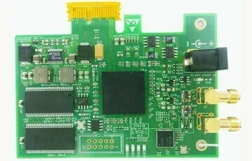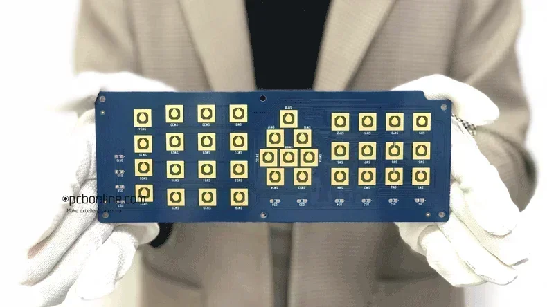
Surface finish selection is critical in printed circuit boards (PCBs). Immersion Gold, or Electroless Nickel Immersion Gold or ENIG, has become the most popular surface finish. Let's examine every aspect and discover why it is the top option for many PCBs.
In this article:
Part 1: Introduction of Surface Finishes Part 2: Overview of Immersion Gold Part 3: The Immersion Gold Process Part 4: Thickness Ranges of Immersion Gold Part 5: Intermetallic Compound (IMC) for Immersion Gold PCB Part 6: Why is Immersion Gold the Most Versatile Surface Finish? Part 7: Immersion Gold PCB Manufacturer One-Stop PCBA ManufacturingIntroduction of Surface Finishes
Understanding that surface finishes is the first step toward exploring Immersion Gold's versatility.
More than just adding visual appeal, these finishes protect copper contacts from corrosion and enhance the soldering procedure. Before delving into Immersion Gold, it is important to understand the wide range of surface finishes.
What are surface finishes?
PCB surface finishes are important layers that protect a printed circuit board's copper contacts. These layers guard against rust, damage, and other outside forces, keeping the board working well for a long time.
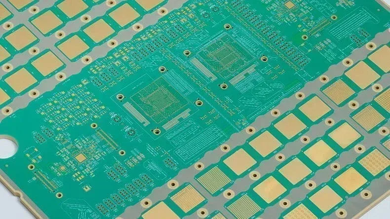
Here are the main types of PCB surface finishes, each with a brief description:
- Hot air solder level (HASL): This common and affordable finish method includes dipping the bare PCB into melted solder. The solder covers the copper, and hot-air knives make the surface even. It works well for big components but isn't great for Fine Pitch Technology because it requires high temperatures and contains lead.
- Lead-free HASL (LF HASL): Like HASL but without lead, LF HASL adheres to RoHS standards. It offers similar functions and pros as HASL but without lead-related concerns.
- Organic solderability preservatives (OSP): OSP creates a thin organic layer on the copper, protecting it from oxidation. It's cost-effective and RoHS-compliant but less durable than other finishes.
- Immersion silver: Silver is deposited directly onto the copper, offering good conductivity and solderability. However, it's sensitive to environmental conditions and requires careful handling. · Immersion tin: Tin is applied via immersion, providing a flat surface for soldering. It's RoHS-compliant and suitable for fine-pitch components.
- Electroless nickel immersion gold (ENIG): A two-layer finish with nickel and gold, ENIG combines good conductivity, solderability, and corrosion resistance. It's widely used for complex PCBs.
- Hard gold plating: A thinner gold layer than ENIG and is electroplated onto the copper surface, hard gold plating provides excellent wear resistance and is suitable for connectors and edge connectors.
- Electroless nickel: A nickel layer without gold, used for wire bonding and aluminum wire bonding.
- Electroless palladium immersion gold (ENEPIG): A three-layer finish with palladium, nickel, and gold, ENEPIG offers robust performance for high-reliability applications.
Remember, choosing the right surface finish depends on your project's requirements and constraints. Each type has advantages and limitations, so consider them carefully when designing your PCB.
Overview of Immersion Gold
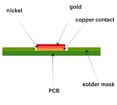
Immersion gold, also called electroless nickel immersion gold (ENIG), is a two-layer nickel and gold protective coating on the copper surfaces of a PCB. Its purpose serves two main functions:
1. Oxidation prevention
When copper traces and plated through holes are uncovered, they can easily become oxidized. Immersion gold acts as a barrier, stopping this oxidation and ensuring the copper stays clean and conductive.
2. Enhanced solderability
Soldering components onto a PCB needs strong connections. The thin layer of gold from immersion gold helps with soldering. It makes a smooth and even surface that makes it easier to create solid solder joints during assembly.
The Immersion Gold Process
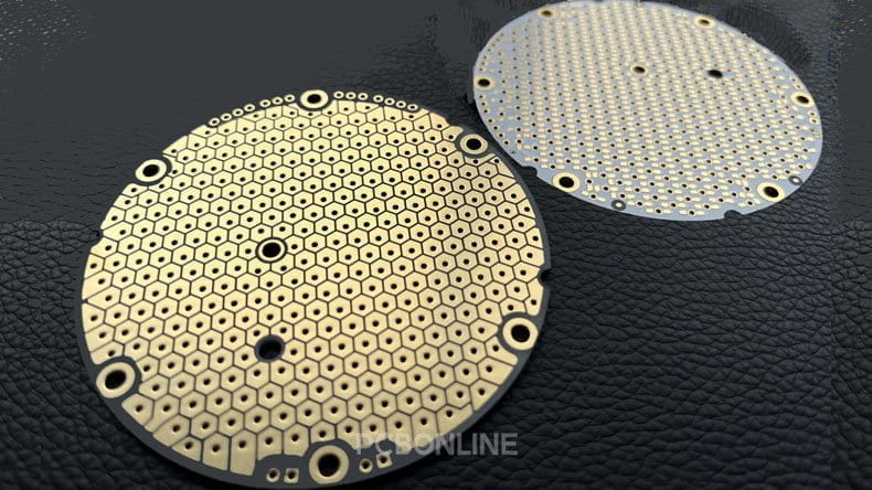
Here's the complete immersion gold process in PCB fabrication.
Step 1. Pretreatment
Objective: Prepare the copper surface for subsequent plating steps.
Process:
- Remove the oxidation layer from copper contacts using chemical solutions.
- Deposit a thin layer of palladium on the copper. This palladium acts as a reducing agent during the immersion nickel process.
Step 2. Immersion nickel
Objective: Transform nickel ions into a solid nickel metal layer.
Process:
- Through a redox reaction, the nickel ions in the solution attach themselves to the exposed copper surfaces.
- This results in a uniform and adherent layer of nickel.
Step 3. Immersion gold
Objective: Transform gold ions into a metallic gold layer.
Process:
- The PCB, now coated with nickel, takes a dip in a gold bath.
- During this quick immersion, gold salts in the solution react with the nickel layer.
- Some nickel oxidizes to Ni²⁺, while the gold is reduced to its metallic state.
- The resulting dual-layer structure—nickel underneath and gold on top—forms the ENIG finish.
Step 4. Post-treatment
Objective: Clean the PCB surface finish and remove residual chemical solutions and moisture.
Process:
- Thorough cleaning ensures that the ENIG-coated board is free from contaminants.
- Drying completes the post-treatment phase.
Thickness Ranges of Immersion Gold
The thickness of each layer varies based on design requirements and cost considerations.
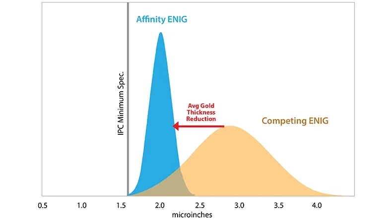
Immersion gold layer: Typically ranges from 1 to 5 microns. Thicker gold layers enhance durability but increase costs.
Nickel layer: Usually falls within the 3 to 6 microns range. Adequate thickness ensures good adhesion and corrosion resistance.
The gold layer on contacts (gold fingers): The gold layer on connectors and edge contacts using immersion gold can be thicker, often exceeding 5 microns.
Remember, the choice of thickness directly impacts the PCB's performance and cost. Designers must strike a balance between functionality and budget when specifying these layers.
Intermetallic Compound (IMC) for Immersion Gold PCB
IMC refers to the compound that forms at the interface between the copper pad on a PCB and the solder materials during reflow soldering. At high temperatures, the surface finish, copper, and solder form the IMC, which marks the success of reflow soldering. Its growth directly impacts the solder joint reliability of immersion gold PCBs.
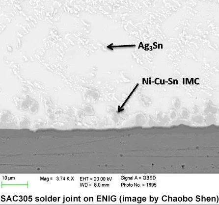
The ENIG Process and IMC
1. ENIG basics:In ENIG, a nickel layer serves dual functions.
- Barrier: It prevents direct interfusion between gold and copper.
- Reaction site: The nickel layer reacts with tin during soldering.
2. IMC formation: The thin nickel layer interacts with the molten solder paste during reflow soldering.
Specifically, the nickel reacts with tin (Sn) in the solder.
The result? The formation of an intermetallic compound, specifically Ni₃Sn₄.
This compound plays a critical role in solder joint integrity.
Why does IMC matter for immersion gold PCB?
In solder joint reliability:
- IMC growth affects the strength and durability of solder joints.
- Too much IMC can lead to joint failure.
- Controlling IMC growth is essential for reliable PCB assembly.
In gold wire bonding:
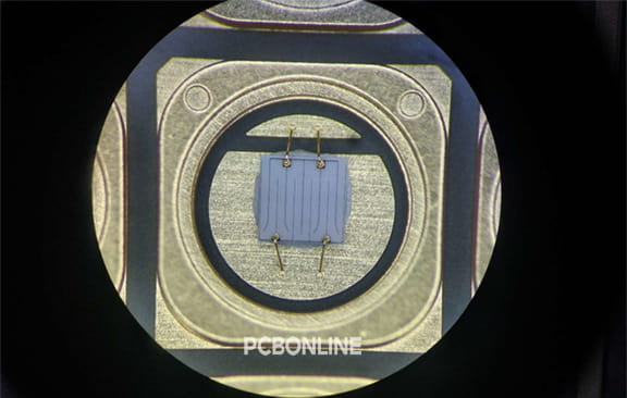
- IMC layers also impact wire bonding, a common technique for mounting IC chips.
- Understanding IMC ensures robust wire bonding connections.
Why is Immersion Gold the Most Versatile Surface Finish?
Immersion gold or ENIG proves its adaptability from rigid to flexible PCBs, showcasing its versatility and strength. It conforms to various PCB types, such as metal-core, ceramic-substrate, FR4, PTFE, and flexible PCBs. This adaptability is a valuable reference for designers in choosing the right surface treatment for a specific board.
Here are reasons for immersion gold's versatility.
Advantages of immersion gold:ENIG's uniformity is not by chance. It meets the demands of fine-pitch assembly, ensuring precise treatment for closely grouped IC pins.
Enhanced reflow soldering:Throughout reflow soldering, the gold layer guarantees effective and dependable solder joints.
Corrosion resistance:ENIG guards against oxidation. Its thin layer of gold protects copper contacts, resisting the corrosive effects of time.
Lifespan prolonged:The PCB, wearing ENIG armor, moves ahead confidently, knowing it will last a long time. Protected by ENIG, it stays strong against rust and time's effects.
Optimized Electrical Performance:Good conductivity: The gold layer of immersion gold has a low contact resistance, leading to good conductivity.
Stable components and current flow:Strong connections ripple through the circuit, harmonizing components and ensuring a smooth current flow.
Reduced skin effect:ENIG lessens the skin effect in high-speed circuits—a quirky electromagnetic interference that can distort signals.
Compatibility with Flexible PCBs:
![]()
ENIG gracefully accommodates the needs of flexible PCBs to bend, flex, and adapt. It effortlessly navigates through the twists and turns of modern designs.
Appropriate for lead-free applications:ENIG aligns with environmental mandates. It adheres to RoHS, the herald of eco-consciousness.
Aesthetic appearance:The gold layer adds a touch of beauty. ENIG combines aesthetics and functionality.
Consistent and reliable:ENIG remains steadfast against environmental changes, serving consistency across various applications. Whether in the Arctic's icy grip or the desert's blazing heat, immersion gold PCB remains unwavering reliability.
In conclusion, immersion gold offers adaptability and many benefits, making it suitable for various PCBs. It's the top choice for high performance and reliability in electronic devices across diverse applications.
Immersion Gold PCB Manufacturer One-Stop PCBA Manufacturing
If you need high-performance PCBs and want to make them PCBAs or final product box-builds, you can select PCBONLINE as your PCBA manufacturer. Whether the PCB uses immersion gold or other surface finishes, PCBONLINE can fabricate and assemble the boards of high quality at one stop.
PCBONLINE was founded in 1999. It has two advanced PCB manufacturing bases, one EMS PCB assembly factory, and an R&D team to provide one-on-one engineering support.
PCBONLINE has independent production lines for gold surface finishes and wastewater treatment equipment.
PCBONLINE has certificates to buy, use, store, and treat gold salt solutions, which are very toxic.
Remember, only high-level PCB manufacturers can complete all immersion gold PCB fabrication and assembly processes, and PCBONLINE is one of them.
Besides immersion gold, all the other surface finishes are accessible for PCB fabrication and soldering at PCBONLINE.
You can have immersion gold PCB manufactured and assembled with any substrates, including FR4, aluminum, copper, PTFE, ceramic, polyimide, and polyester.
All the PCBs, PCBAs, and box-build assemblies made by PCBONLINE are certified with ISO 9001:2015, IATF 16949, RoHS, REACH, UL, and IPC.
The experts from PCBONLINE can choose appropriate layer thicknesses of immersion gold for your board and optimize your design. Whether you have completed the immersion gold PCB design or not, you can work with PCBONLINE providing all-around electronic manufacturing. If you want to send your inquiry to PCBONLINE, please contact by email at info@pcbonline.com.
Conclusion
Immersion gold is a versatile surface finish for printed circuit boards due to its many benefits. This article illustrates the layers, thickness ranges, and IMC of immersion gold, it also briefly introduces the other surface finishes for your boarder understanding. Additional research studies can enhance the professionalism of immersion gold, and you can chat with the experts of PCBONLINE from the online chat window.
PCB fabrication at PCBONLINE.pdf


