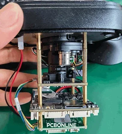
IoT embedded system for smart transportation cameras
An embedded system lies in many Internet of Things (IoT) devices. As the smart electronic market keeps growing, the embedded systems in IoT are becoming the backbone of the larger IoT systems or devices.
In this article:
Part 1. What is an Embedded System in IoT? Part 2. IoT Embedded Systems Applications Part 3: HDI PCBs for IoT Embedded Systems One-Stop PCBA Manufacturer for IoT Embedded SystemsPart 1. What is an Embedded System in IoT?
IoT embedded systems are specialized computer systems combined with hardware and software components to execute certain functions under minimal human interference and integrate them into a larger system or IoT device. An embedded system typically consists of hardware components like microcontrollers, sensors, and actuators. Specialized software is programmed into read-only memory (ROM) or flash memory to perform its functions.
Below are the functions of IoT embedded systems.
- Data acquisition and processing: Embedded systems collect data from sensors (e.g., temperature, humidity) and process it to derive insights. It enables devices like smart thermostats to optimize energy usage.
- Connectivity and communication: IoT embedded systems facilitate communication between IoT devices and networks, using protocols like Wi-Fi, Bluetooth, and MQTT. It allows devices to interact and connect to cloud services.
- Sensing and actuation: Embedded systems integrate sensors to detect environmental changes and actuators to respond. For instance, smart homes use sensors to detect motion and trigger lights or adjust temperature.
- Real-time processing: IoT systems quickly collect and process data, allowing fast actions like adjusting temperatures, detecting problems, or triggering alarms based on sensor readings.
The embedded systems are used in many IoT applications, such as smart household appliances, complex industrial machinery, and medical devices.
Part 2. IoT Embedded Systems Applications
Iot embedded systems silently work behind the scenes to enhance our lives in countless ways. They are used in many IoT fields.
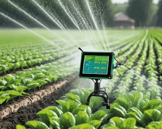
Smart agriculture irrigation
IoT-embedded systems such as smart irrigation can be used in smart agriculture. It automates watering based on soil moisture and weather conditions to conserve water. The system reduces water wastage and ensures that crops are watered only when necessary.
The IoT-embedded system for smart irrigation includes:
- Soil moisture sensors (for collecting data)
- ESP32 microcontroller (for processing sensor data and controlling irrigation)
- Water pumps (activated by relays)
Energy monitoring
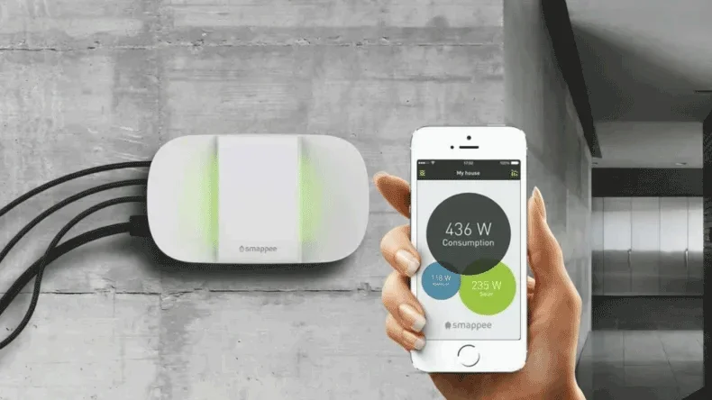
IoT-embedded systems can be used in energy monitoring. It helps monitor and manage energy consumption in real time. The goal is to reduce electricity usage and improve efficiency.
The IoT-embedded system for energy monitoring includes:
- Current and voltage sensors (for measuring energy usage)
- Raspberry Pi or Arduino (for aggregating and analyzing the data)
- Web interface or mobile app (for displaying information and providing energy-saving tips)
Smart waste management system
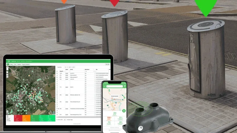
The IoT-embedded system can be used for smart waste management. It optimizes waste collection and disposal by monitoring trash bin fill levels in real-time, ensuring timely pickup and reducing waste collection costs.
The IoT-embedded system includes:
- Ultrasonic sensors (for measuring the fill level of trash bins)
- Arduino or ESP32 (for processing the sensor data and managing the communication)
- Mobile app or web dashboard (for monitoring waste levels and scheduling pickups)
Besides, IoT-embedded systems are used in industrial cameras for smart transportation monitoring, smart security in customs gates, etc.
Part 3: HDI PCBs for IoT Embedded Systems
An IoT-embedded system is a PCBA (printed circuit board assembly) that carries and connects various components. As IoT and AI technologies grow, the circuitry gets more and more sophisticated, and High-Density Interconnect (HDI) PCBs are used for IoT embedded systems.
HDI PCBs are used in the IoT and AI electronics to make devices smaller and more multifunctional. They provide a high number of connections in a tiny space. This is achieved through advanced technologies such as microvias and serial lamination.
The Vias in HDI PCBs
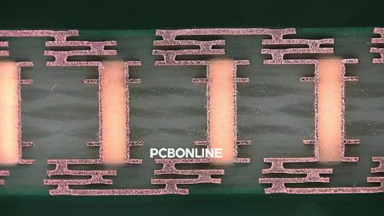
Vias are copper-plated holes that connect different layers of a printed circuit board (PCB). In HDI technology, there are four main types of vias:
- Through-hole vias: They go all the way from the top to the bottom layer. They are easy to make but take up more space.
- Buried vias: They are only found inside the board and connect two or more inner layers. They are not visible from the outside, which helps keep the surface clean.
- Blind vias: They connect an outer layer to one or more inner layers without going all the way through. They save space and are useful for complex designs.
- Microvias: They are very tiny holes (diameter < 0.15mm) that allow for dense connections. They help designers create detailed patterns that larger vias cannot.
Signal integrity
Signal integrity is important to HDI PCBs in IoT embedded systems. It refers to how well electrical signals maintain their quality as they travel through the PCB. To keep signals clear and strong, HDI PCBs use:
- Shorter paths: By minimizing the distance signals have to travel, they reduce delays and interference.
- Controlled impedance: By designing for standard values like 50 ohms for single-ended traces and using simulation tools, HDI PCBs have a consistent electrical resistance, which prevents signal reflections that can cause data errors.
HDI PCB materials
The materials used in HDI PCBs affect their performance:
- FR-4: This is the most common material for HDI PCBs for IoT embedded systems used for low to medium-complexity devices like wearables. It's affordable and works well for many applications.
- Rogers and PTFE materials: Used for high-frequency IoT applications like RF sensors and IoT hubs. They perform better than FR-4 and maintain signal quality.
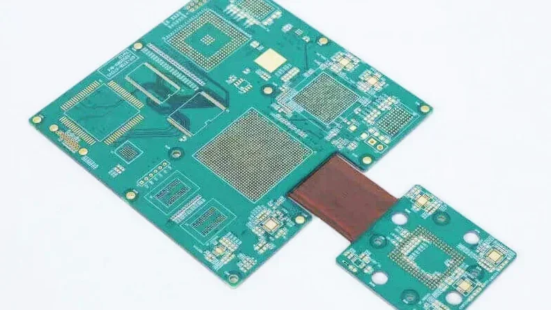
- Polyimide materials: Flexible and rigid-flex HDI PCBs use these materials. They are bendable and are suitable for compact designs that require 3D flexibility.
Stack-up design
An HDI PCB has at least 4 copper layers in the 1+2+1 stack-up, including:
- Top layer: Signal layer with components
- Inner layer 1: Ground plane
- Inner layer 2: Signal layer
- Bottom Layer: Ground plane or another signal layer
For controlling impedance, the ground/power planes are close to signal layers to control capacitance and inductance. This setup allows for effective routing while keeping signals protected.
Why choose HDI PCBs for IoT embedded systems?
HDI PCBs are widely used as the backbone of IoT embedded systems because of these advantages:
- Compact design: With microvias and fine traces, HDI boards can house more components in less space, which is essential for sleek embedded systems in IoT.
- Superior signal integrity: Shorter paths between components reduce delays and interference, making HDI PCBs ideal for IoT devices with communication functions.
- Multilayer and lightweight: IoT devices especially AI and AR devices integrate many functions in a small gadget, such as sensors, processing, and communication. The HDI PCBs with a high layer count (up to 64 layers) provide enough design space. Besides, compared with other devices with the same multi-functions, HDI PCBs are lightweight and take less space.
One-Stop PCBA Manufacturer for IoT Embedded Systems
If you want custom electronics manufacturing from R&D, PCB, to finished IoT devices under one roof, you can work with the one-stop IoT PCBA manufacturer PCBONLINE.
Found in 1999, PCBONLINE has two large advanced PCB manufacturing bases, one PCB assembly factory, stable supply chains, and an R&D team for development and one-stop PCBA manufacturing for IoT embedded systems.
PCBONLINE has R&D capabilities and rich IoT embedded system development experience. We can do the R&D or take part in your project's development from the early stages.
PCBONLINE offers free design for manufacturing (DFM) and one-on-one engineering support and solves all technical issues to ensure the smooth manufacturing process and successful results of your IoT project.
Strong and one-stop IoT PCBA manufacturing capabilities custom meeting your requirements, including R&D, prototyping/sampling, PCB fabrication, component sourcing, PCB assembly, PCBA value-added, and IoT device box-build assembly.
PCBONLINLE has strategic cooperation with Espressif for sourcing the IoT chips and the top 3 mold and enclosure manufacturers in China for manufacturing high-quality jigs and enclosures.
As a source factory manufacturer for PCBA and IoT embedded systems, the electronics manufacturing from PCBONLINE is at reasonable prices without hidden costs.
To get a quote for your IoT embedded system PCBA project, please contact info@pcbonline.com. When your project goes to bulk production, we will refund the fees of R&D, sampling, and PCBA functional testing to you.
Conclusion
IoT embedded systems provide real-time monitoring and data exchange, remote control, etc, to the larger IoT system or device. They find wide applications in all the IoT fields, including smart homes, medical, industrial, agriculture, smart city, transportation, and environmental monitoring. To bring your IoT embedded system project into real boards and devices, chat with the one-stop IoT PCBA manufacturer PCBONLINE from the online chat window.
PCB assembly at PCBONLINE.pdf


