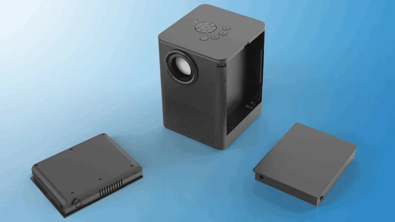
The Internet of Things brings physical objects into the digital world, and the IoT hardware is the bridge that connects the two worlds: physical and digital. The bridge connection is based on collecting, sharing, communicating, and taking action on data in which IoT hardware plays a vital role.
In this blog, you will gain insight into IoT hardware development.
We will understand IoT hardware and discuss the development process, from initial idea to mass PCBA production.
In this article:
Part 1: Introduction to IoT Hardware Part 2: Key Components of IoT Hardware Part 3: The IoT Hardware Development Process Part 4: IoT Hardware Building From R&D to Massive PCBA Box BuildsIntroduction to IoT Hardware
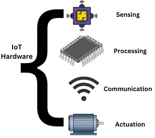
IoT hardware represents the physical components of IoT devices, encompassing sensors for data collection, microcontrollers for processing, and communication modules for data exchange.
These components connect objects to the internet, enabling them to interact with their environment and transmit valuable information.
The IoT hardware combines with other essential IoT components to transform ordinary objects into smart devices.
Key Components of IoT Hardware
The IoT hardware comprises several key components that work together to achieve the functionalities mentioned in the previous section.
Microcontrollers and Microprocessors
Microcontrollers and microprocessors are the most important components of IoT hardware. Microcontrollers are mainly used in simpler applications due to their compact size and lower power consumption, on the other hand, microprocessors, like those found in Raspberry Pi devices, offer greater processing power for more demanding tasks.
Both are responsible for processing data received from sensors and controlling the actions of the device based on programmed instructions. Based on the requirements either of them or both are used in the project.
Following are some of the development boards which contain microcontrollers or microprocessors used for IoT development:
- ESP32 and ESP8266
- Various Arduino boards
- Raspberry Pi Pico
- NRF and STM-based microcontrollers
- Raspberry pi
Sensors and Actuators
Sensors and actuators are the main components in IoT hardware development. Sensors gather information from the environment, like temperature or motion, while actuators perform actions based on that information or instructions from the processing unit.
For example, a sensor could detect soil moisture value, triggering an actuator to water the plants.
Communication Modules
Communication modules in IoT hardware development provide the circuitry for devices to connect and transmit data using various communication protocols. These modules can include wireless technologies such as Wi-Fi, Bluetooth, and cellular, or wired interfaces like USB and CAN. The choice of communication module depends on factors like range, data rate, power consumption, and security requirements.
Most of the microcontrollers and microprocessors discussed in the previous section have built-in WiFi and BLE modules, widely used communication methods.
Other communication methods such as LoRa, Zigbee, and cellular communication require interfacing using external communication modules.
The IoT Hardware Development Process
The process of IoT hardware development is not a very strict process. The following steps are involved in developing the IoT hardware.
Outline the idea
This initial phase, called ideation and conceptualization, involves pinpointing the problem or opportunity the IoT product aims to address. We define the target audience, value proposition, and core features that are critical in this step.
For example, a problem can be inefficient water usage in irrigation, which leads to over or under-irrigation. To solve the problem, we will need to optimize the water usage and real-time monitoring and the target audience will be mostly farmers.
Conduct product research
This product research is crucial to validate the idea and ensure its viability. Thorough market research helps understand the competitive landscape, user needs, and potential challenges.
For our water optimization project, we can research the current irrigation solutions and their success, we can find the gaps in the current solutions and we can analyze the farmer needs and potential connection challenges.
Map out a preliminary hardware design
This initial hardware design bridges the gap between the concept and the actual design. We specify electronic functions, and their interconnections, and select key components as discussed in the previous section. It is important to set the stage for subsequent design phases.
For our project, we can select sensors such as soil moisture, temperature, humidity, and water flow sensors. We can select the controller and communication module and design a mind map based on their interactions.
Schematic design
Then we create a detailed schematic circuit diagram that provides a visual blueprint of the electronic component interconnections within the IoT device.
The schematic diagram is essential for ensuring accurate connectivity and functionality and serves as a guide for PCB layout design and component selection.
Now for the water optimization project, we can create a schematic design with actual connections, highlighting the proper functionalities and interfacing.
PCB design
We will use CAD tools to convert the schematic diagram into a physical Printed Circuit Board (PCB) layout. This step involves carefully considering size constraints, power consumption, and signal integrity because a lot of complexity is involved in PCB design, particularly for products with wireless connectivity.
Generate the final Bill of Materials (BoM)
The BoM is a comprehensive list of all components, including their specifications and quantities, required for building the IoT device.
For our project, we will now create a list of all the components such as sensors, controllers, speakers, and other components. This helps manage inventories, especially in cases like semiconductor chip shortages in 2020-2023.
Prototyping
Building a prototype allows for testing the hardware and software integration. The PCBA prototype utilizes development boards, 3D printing for enclosures, and integration of sensors and actuators. It is very important to measure the feasibility of the product and to ensure a quick and easy development process.
For our project, this step will allow us to test our circuit by evaluating each component individually and all of them together.
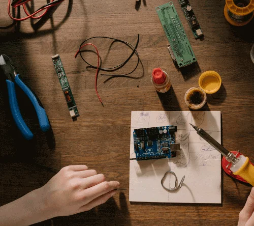
Fig: Prototyping and Testing IoT Hardware
Firmware development
We will develop the firmware that runs on the device's microcontroller which is essential for controlling hardware interactions, communication protocols, power management, and security features.
System Integration
System integration involves combining all hardware and software components into a fully functional system. It addresses compatibility issues and ensures seamless data flow and communication between various modules.
This stage will allow us to test our irrigation project and find out the possible issues, such as the complete system testing in the real environment.
Software development
We will then develop software applications for user interfaces, backend systems, and cloud platforms that interact with the IoT device that is crucial for data visualization, analysis, and remote control.
For our project, we will make sure that the interface is well-suited for our target audience.
Cloud development
Establishing a robust cloud infrastructure for data storage, processing, and analytics is paramount. Choosing a reliable cloud service provider offering scalability and security features is critical.
For example, in our project which is located at a remote location, we can consider TTN (the things network) and services of some full-fledged clouds such as AWS, Azure, and GC.
Comprehensive testing
This step involves functional testing, performance testing, stress testing, security testing, and user acceptance testing.
This step can be the beta version of our water optimization project, where everything will be tested and we collect the data for improvements.
Improvements
Based on testing results and user feedback, iterative improvements to hardware, firmware, software, and cloud infrastructure are implemented to enhance the product's quality and usability.
Design for manufacturing and assembly
Optimizing the design for streamlined production by simplifying complexity and reducing costs is critical before mass production. DFMA focuses on minimizing assembly steps and using standardized parts.
Mass production
The final step involves moving into mass production after all tests and design refinements are complete. Maintaining consistent quality control during the manufacturing process is vital.
The process involves research, prototyping, selecting components, designing the circuit board, developing firmware, and testing everything thoroughly. Finally, mass production happens, making sure quality stays high throughout.
IoT Hardware Building From R&D to Massive PCBA Box Builds
If you have completed IoT hardware development, you will need PCBA manufacturing services to build your IoT project into real devices. PCBONLINE, a one-stop IoT hardware builder, can provide you with turnkey PCBA manufacturing from R&D and prototypes to mass PCBA box build assembly.
Founded in 1999, PCBONLINE has two large advanced PCB manufacturing bases, one PCB assembly factory, stable supply chains, and an R&D team for IoT hardware development and manufacturing.
PCBONLINE has strong IoT development expertise and can do the R&D for your IoT project according to your initial idea and specs requirements, including software and hardware, or take part in your IoT project development from the early stage.
PCBONLINE offers free prototype/sample, PCBA functional testing, and design for manufacturing (DFM) for massive production IoT projects.
One-stop IoT PCBA manufacturing services for IoT hardware building from ideas to end devices, including R&D, prototypes, PCB fabrication, component sourcing, PCB assembly, PCBA value-added, enclosures, box-build assembly, and application simulation testing.
High-quality IoT PCB and PCBA manufacturing certified with ISO 9001:2015, ISO 14001:2015, IATF 16949:2016, RoHS, REACH, UL, and IPC-A-610 Class 2/3.
We offer one-on-one engineering support no matter what quantity of PCBA you want until delivery. To get a quote for your IoT project, please contact info@pcbonline.com.
Conclusion
IoT hardware development involves creating a physical product from an idea after going through many steps. You need to understand what users want, plan carefully, and keep making things better. The IoT hardware development process can be challenging, such as managing power consumption, securing the device against threats, and designing for scalability. All R&D issues can be tackled with the one-stop IoT hardware builder PCBONLINE, and don't hesitate to chat with us from the online chat window.
PCB assembly at PCBONLINE.pdf


