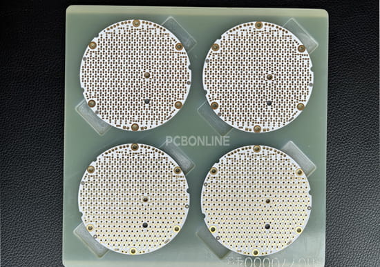
Recently, the PCBONLNIE team received the same question from some customers, how do we depanel round ceramic PCBs?
We use laser-cut to depanel ceramic PCBs.
Why laser depaneling ceramic PCBs? Ceramic PCBs (alumina PCBs and aluminum nitride PCBs) are hard and fragile, and laser cutting is the best way for ceramic PCB profiles.
You will know about laser depaneling ceramic PCBs from the below content.
Part1: What is Laser Depaneling PCB
As you know, PCBs are not manufactured piece by piece but panel by panel. Here, the panel means a large production panel, where several PCB boards are grouped for manufacturing and assembly. After PCB assembly, we cut the PCBs from the panel, and this process is called PCB depaneling.
![]()
Laser-cut is a PCB depaneling method apart from V-cut and computer numerical control (CNC). It is especially used for ceramic PCB depaneling or profile.
During ceramic PCB manufacturing, the laser cuts the ceramic substrate according to the designed lines and width for the PCB profile, so that the boards can be easily separated from the panel after the SMT assembly.
Part 2: How do We Depanel Ceramic PCB PCBs
Alumina PCBs and aluminum nitride PCBs can't be cut by CNC or V-cut, because the CNC machine and V-cut machine either don't have the power to cut ceramic or can break the ceramic boards. We need to use the controllable laser to depanel ceramic PCBs. The cutting direction and width are set up before depaneling.
![]()
Before laser cutting the ceramic PCB panel, our engineers design the PCB panelization and reserve the PCB craft edges.
When PCB panelization is designed, we set up the laser specifications according to the designed separation lines and width. Usually, our engineers retain one-third of the PCB board thickness along the separation lines on the panel.
![]()
During ceramic PCB fabrication, the automatic laser cutting head moves over the ceramic panel in the shape of designed depanelization lines, and 2/3 of the ceramic thickness is removed from the desired separation lines.
After the laser head goes through above the panel, we clean and remove the carbon on the panel.
Laser-cut or PCB profile is the final step in ceramic PCB manufacturing. Then the PCB panels are put on a custom-made tray and sent to the SMT assembly lines for surface-mounting components.

Laser depaneling PCB enables ceramic PCBs to be surface-mounted in panels. After the SMT assembly, our technicians can break off the separation lines with only a pair of pliers.
Part 3: Laser Depaneling PCB vs Diamond Cut PCB Depaneling
Before the comparison between laser depaneling and diamond-cut depaneling, I need to introduce diamond-cut PCB depaneling. It is the other ceramic PCB depaneling method, which is similar to V-cut because it happens at room temperature and the line has to be straight. It uses a diamond cutter to depanel ceramic PCBs.
Both the two ceramic PCB depaneling methods are applied by PCBONLINE. Here are the differences we conclude from ceramic PCB manufacturing.
- Depaneling PCB shape differences- a laser can depanel round ceramic PCBs, while a diamond cutter can depanel only rectangular ceramic PCBs.
- Depaneling PCB temperature differences- laser generates much heat, and the temperature is high, while diamond depaneling PCB doesn't generate heat.
- Carbonization differences- the laser will cause carbonization on the ceramic materials, so cleaning is necessary to remove the carbon, while diamond-cut PCB depaneling doesn't cause any carbonization.
From the above, you can see that round ceramic PCBs can only be depanelized by laser. We suggest designing rectangular-shaped ceramic PCBs because their panelization and assembly are easy.
How about rounded ceramic PCBs? No worry about SMT assembly if your ceramic PCB is rounded.
At PCBONLINE, we provide free trays for rounded ceramic PCBs so that they can be surface-mounted.
Here is an example of trays for rounded aluminum nitride PCBs depaneled by laser cut.
One-Stop Ceramic PCB Manufacturing - PCBONLINE
The above content introduces how we, the PCBONLINE team depanel ceramic PCBs. PCBONLINE is an advanced PCB manufacturer founded in 1999. We have two large PCB manufacturing bases and one PCB assembly factory that are ISO and IPC certified.
![]()
In PCB profiling, we depanel ceramic PCBs by laser or a diamond cutter. For HDI PCBs, aluminum PCBs, high-frequency PCBs, rigid-flex PCBs, etc, our PCB depaneling methods include V-cuts, CNC, and half-holes.
If you are looking for a ceramic PCB manufacturer, here are reasons for you to consider PCBONLINE:
- PCBONLINE provides all kinds of ceramic PCBs and products, such as alumina PCBs, aluminum nitride PCBs, IGBT ceramic substrates, UVA modules, etc.
- Ceramic PCB prototypes, batch manufacturing, and assembly have no quantity limit.
- We adopt the DPC technology to realize 3D ceramic PCB design into reality.
- Minimum trace space/width of 20μm, conductive layer thickness arbitrarily customized from 1μm to 1mm.
- Free one-on-one engineering support (DFX) throughout your ceramic PCB project.
All ceramic PCBs from PCBONLINE are depaneled by laser. Please feel free to send your Gerber/IPC-2581/BOM to PCBONLINE if you have manufacturing needs.
Conclusion
Laser depaneling PCB is necessary for ceramic PCB manufacturing. It eases ceramic PCB SMT assembly and separates PCBs off the panel after assembly. If you have demands for ceramic PCBs/PCBA, don't miss the 23-year-old source factory PCBONLINE.


