
Printed circuit board (PCB) plays an essential part in countless electronic gadgets ranging from smartphones, and car systems, to space technology.
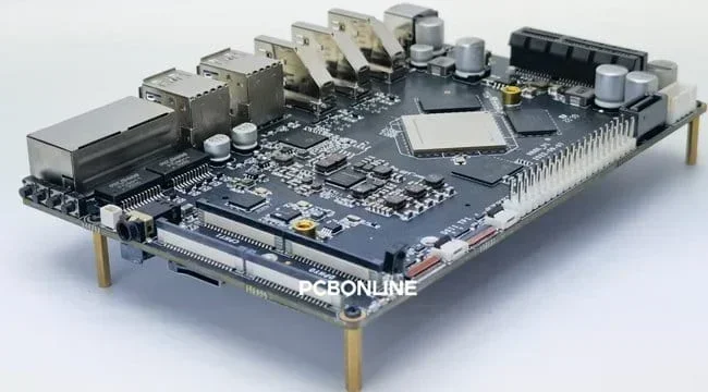
When a PCB has components attached to it, we refer to it as a PCBA, and the creation process is known as printed circuit board assembly or PCB assembly.
Let's dive further to explore more about PCB assembly.
What is A Printed Circuit Board Assembly?
Printed Circuit Board Assembly, often shortened to PCB assembly, is a process of attaching electronic parts onto a blank PCB.
PCB assembly is a delicate act of introducing electronic components to a PCB, which eventually results in a reliable and functioning circuit board.
Essentially, a PCB is a semi-finished product that mounts components so that it can function as an electronic product. After further assembly, the PCBA becomes a finished product.
The PCB assembly process includes SMT (surface-mount) and THT (through-hole) assembly.
SMT assembly means picking and placing SMDs (surface-mount devices) on the PCB pads and then reflowing solder to attach the SMDs to the PCB.
THT assembly means inserting the leads of the THT components through PCB holes and then a wave solder to connect the THT component to the PCB.
Each step of PCB assembly demands thorough attention to detail to guarantee product performance, reliability, and fidelity to the planned specifications.
Overview of the PCB Assembly Market
The PCBA market plays a pivotal role in the electronic industry's growth, as all electronic products require PCB assembly.
PCB assembly involves many companies, including PCB/PCBA manufacturers, original equipment manufacturers (OEM), electronic component suppliers, and PCBA material suppliers (such as laminates used in PCB fabrication and solder paste used in PCB assembly).
The growing demand for consumer electronics, automotive electronics, industrial automation, and the Internet of Things (IoT) have fueled the growth of the PCBA industry.
Plus, tech advances and the increasing need for smaller, more efficient, and high-performing electronic products have escalated the demand for sophisticated PCB assembly.
PCB Assembly Technologies and Trends in 2023
In PCB assembly, there are two technologies — SMT and THT.
Surface-Mount Technology (SMT)
Surface-mount technology is the mainstream PCB assembly technology. It is automatic and efficient.
SMT offers benefits like smaller component sizes, enhanced production efficiency, and cost savings.
The components used in SMT assembly are SMDs, which have short pins or solder balls. They are attached to the PCB pads by the cured solder paste.
The move from through-hole technology to SMT has been stimulated by the need for tinier PCBAs and heightened functionality.
Though-Hole Technology (THT)
Through-hole technology is the earliest-developed PCB assembly technology. It is half-automatic.
If your project aims for small-batch production, you can design through holes on the PCB to mount components, as THT assembly is more cost-effective than SMT for low-volume PCB assembly.
The trends molding the PCBA market include:
- Downsizing and high-density designs: The shift towards smaller and lighter electronic gadgets has spurred a need for high-density PCBA. Engineers stretch the limits of PCB design to house more components, resulting in heightened integration and complexity.
- IoT and Industry 4.0: IoT and the notion of Industry 4.0 paved paths for PCBA. As devices become more interconnected and communicative, the demand for smart PCBAs has risen. This trend boosts the demand for IoT-compatible PCBA and sensors.
- Automation and robotics: For higher PCBA quality and volume, PCBA manufacturers are turning to automation and robotics in PCBA procedures. Automated pick-and-place machines, automated inspection systems, automated guided vehicles, and so on are put in use.
- Environmental factors: The electronic industry is growing more conscious about environmental sustainability. This awareness resulted in the use of lead-free solder, components, and the entire PCB assembly services in PCBA manufacturing.
PCB Assembly Process
The Printed Circuit Board Assembly (PCBA) process is an intricate procedure involving meticulous attention to detail. Here's a step-by-step PCBA process:
DFM and DFA
Before PCB manufacturing and assembly, the PCB design undergoes a design evaluation via Design for Manufacturing (DFM) and Design for Assembly (DFA). DFM and DFA spot potential errors to ensure manufacturability, functionality, and lifespan.
PCB fabrication
This is the transition from design to physical reality. PCB fabrication adheres to specific standards.
The PCB fabrication process involves cut laminate > inner layer circuits > lamination > drilling > copper plating > outer layer circuits > surface finish > solder mask and silkscreen > profile > testing.
Solder paste printing
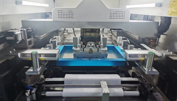
A process where solder paste is precisely applied to the PCB pads. The procedure includes SMT stencil preparation, alignment, and paste deposition. This forms the solder joints necessary for the PCB assembly.
On an SMT line, the blank PCB piled up in a machine called a loader is transferred into a solder paste printing machine.
Here a scraper carrying solder paste presses on the SMT stencil, and the solder paste passes through the stencil holes and is printed on the PCB beneath the stencil.
Solder paste inspection (SPI)
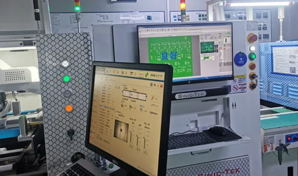
An in-line inspection that ensures the quality of the solder joints.
The inspection machine scans the solder joints and compares them with the reference. The inspected parts include the thickness, position, and size of the solder paste on the PCB pads.
Pick and place
This procedure employs robotic devices to place SMDs onto the solder joints accurately.
The pick and place machines are equipped with component data from the PCB design files, set up component feeders, pick up components, place them in the specified locations, and ensure high placement accuracy.
The pick-and-place machines include high-speed mounting and functional mounting machines.
The high-speed mounter picks and places SMDs in small footprints such as resistors, capacitors, and inductors.
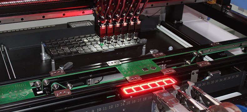
The functional mounter picks and places SMDs in larger footprints such as ICs, connectors, and BGAs.
X-ray inspection
If it is the BGA PCB with solder balls that is to be reflow soldered, we have to inspect them with an X-ray before reflow. This ensures the PCB functionality.
Reflow soldering
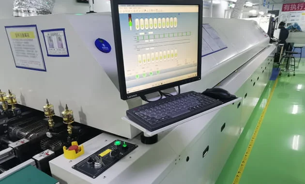
After placement, the PCB enters a reflow oven, which is melting and then cooling the solder paste in a controlled environment.
In the reflow oven, the reflow soldering process includes:
- preheating the entire PCB >
- baking to melt the solder paste >
- flux in the solder paste is separated out to activate the soldering and evaporates away >
- reflow reaches a peak and stays for 10–20 seconds, where the SMD leads and the solder forms an IMC (intermetallic compound) >
- start of cooling down >
- the IMC solder joints cure and form permanent connections between components and the PCB.
Inspection and quality control
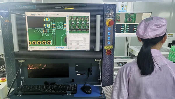
Post-soldering, an automated optical inspection (AOI) takes place.
The PCBA passes through the AOI machine, where the infrared cameras scan the surfaces of the PCBA and take hundreds of images in a second.
The AOI machine compares the images with the reference of the design files and spots the errors if there are any.
Through-hole component insertion
Depending on the PCB type, it may have through-hole components.
The leads of the THT components are manually or automatically inserted through the PCB holes.
Wave soldering or selective soldering
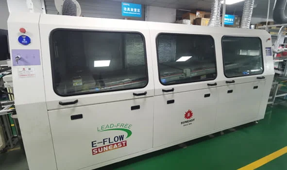
This step solders the THT components onto the PCB.
Depending on the PCBA requirements, wave soldering or selective soldering is utilized.
In wave soldering or selective soldering, the PCBA is:
- preheated >
- sprayed with flux >
- wave soldering: the PCBA placed in a jig is soaked in the liquid tin waves so that the gaps between the PCB hole walls and component leads are filled with solder.
- Or selective soldering: a spay head with a nitrogen protection device solders the PCB holes one by one to form permanent connections between the hole wall copper and the component leads.
After the soldering, technicians trim the THT component leads to be 1–2mm long and clean the PCBA to remove any flux residue.
Post-assembly testing and value-added
To ensure proper assembly, a functional test is conducted.
The PCBA is placed on a jig-testing machine that powers on to test the electrical functions of the PCBA.
Besides, the post-assembly tests include thermal aging and an application stimulation test.
The post-assembly services include IC programming, conformal coating, and box-build assembly.
- Thermal aging: powering up the PCBA for 24–148 hours. It ensures the durability of the PCBA after long working hours.
- IC programming: transferring a program into an IC. It can be done by downloading the program to the local computer and transferring it to the IC or sending the program to your private cloud and transferring it to the IC directly.
- Conformal coating: spraying a protective coating on the PCBA. It protects the PCBA from chemicals, moisture, vibration, and dust and lengthens its lifespan.
- Box-build assembly: installing wire cables and an enclosure to the PCBA to make it a finished product. After that, the PCBA manufacturer labels and packages the end products.
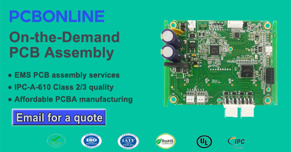
One-stop PCB Assembly on-the-Demand
PCBONLINE is a one-stop PCB manufacturer and assembler for middle and high-end applications, such as automotive, medical, communication, military, computing, industrial, and consumer electronics.
Founded in 1999, PCBONLINE has two large advanced PCB manufacturing bases and one PCB assembly factory.
It takes part in co-procurement with other EMS for components so that the components from PCBONLINE are traceable, quality, and cost-effective.
By working with PCBONLINE, you can have PCBA manufactured with the best quality meeting your requirements:
- PCBONLINE independently finishes the entire PCB fabrication, PCBA, and post-assembly testing and value-added services.
- The PCBA manufacturer PCBONLINE provides on-demand PCB assembly from prototypes to mass production.
- Besides DFM, DFT, DFA, and DFX, the professionals from PCBONLINE provide one-on-one engineering support throughout your project.
- The PCB and PCBA manufacturing at PCBONLINE follows high-quality IPC class 2/3 standards and is certified with ISO, IATF, REACH, RoHS, UL, and IPC.
- PCBONLINE offers free PCBA samples and functional testing for bulk production orders.
If you work for an OEM, research institute, or maker business, the one-stop PCBA manufacturing from PCBONLINE can meet the production demands of your products. Please feel free to reach out to PCBONLINE by email at info@pcbonline.com.
Summary
This blog gives an introduction to printed circuit board assembly, trends in the PCBA market, PCB assembly technologies, and the PCB assembly process. The increasing demand for compact and high-performance PCBs, along with the push towards sustainability and increased automation, shape the evolution of PCBA. If you have any PCB assembly or electronics manufacturing plan and need a reliable PCBA supplier, talk to PCBONLINE from the online chat window on the right.


