
PCB buttons are momentary push buttons. From consumer devices to industrial and medical equipment interfaces with metal domes, PCB buttons provide quick, responsive, and intuitive input. While they may seem like small components, their design significantly impacts functionality, durability, and even user experience.
In this guide, we'll explore the different types of PCB buttons, how to design their pads, how surface finishes like carbon ink and hard gold affect performance, and what to consider when designing PCB power buttons. We'll also touch on mechanical aspects, including button height and support features that ensure long-term reliability.
In this article:
Part 1. PCB Buttons vs. PCB Switches Part 2. PCB SMD Buttons vs. PTH Buttons Part 3. Button Height and Enclosure Design Part 4. Designing PCB Button Pads Part 5. Surface Finishes for SMD Buttons Part 6. Special Case: PCB Power Buttons Turnkey Button PCB Manufacturer PCBONLINE from PCB to Enclosure AssemblyPCB Buttons vs. PCB Switches
First, it's worth clearing up a common confusion: PCB buttons and PCB switches are not exactly the same.
- A PCB button is a momentary switch. It only completes a circuit while being pressed and returns to its original state once released.
- A PCB switch, on the other hand, is a broader category. It includes all types of mechanical or electronic switching mechanisms mounted on a PCB, including toggle, slide, rocker, and DIP switches, many maintain their state until toggled again.
PCB SMD Buttons vs. PTH Buttons
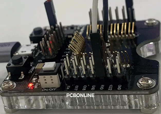
PCB buttons come in three main mounting styles: Surface Mount Device (SMD), Plated Through Hole (PTH), and contact pads. Each has its pros and cons, depending on the application.
SMD buttons
SMD buttons are picked and placed to mount onto the surface of the PCB. They're compact, compatible with automated assembly, and well-suited for space-constrained designs.
Pros:
- Smaller footprint, great for slim or portable devices.
- Can be placed and soldered during the standard reflow process.
- Available in various heights, making them flexible for different enclosure designs.
Cons:
- Less mechanically robust. They are soldered on the PCB surface and can be vulnerable to repeated mechanical stress.
- Need mechanical support adding extra pads around the button helps anchor it better and absorb force during use.
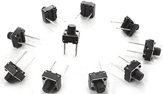
PTH buttons
PTH buttons have leads that go through the PCB and are soldered from the other side. This gives them a stronger mechanical bond. The choice between SMD and PTH depends on your project's needs compact design and automated assembly favor SMD, while rugged, high-use applications are a better fit for PTH buttons.
Pros:
- Very durable and better at handling mechanical stress.
- Good for applications where the button will be pressed frequently or forcefully.
Cons:
- Larger and take up more PCB space.
- Slower and more expensive to assemble compared to SMD, especially in automated production lines.
Contact pads
Contact or button pads are designed on the PCB to form conduction through mechanical contacts or human contact, without soldering physical buttons. They include:
Mechanical contact buttons like silicon rubber keypads are used for remote controls.
Capacitive/resistive touch buttons are used for touch screens and smart homes.
Pros:
- No soldering and low cost.
- Highly durable (> 1 million times).
- Dustproof and waterproof.
Cons:
- Easy to touch by mistake.
- No clear press feedback. Users may need visual or audio cues to confirm whether they have pressed.
No matter what button type is, after a PCB is assembled with a button, the PCB button is tested in the post-assembly stage. The button strike life test ensures the PCB button can withstand the expected press-to-go times.
For most projects, SMD buttons with proper support pads offer a good mix of space-saving design and functionality. If your design demands high durability, PTH buttons or reinforced support structures may be a better fit.
Button Height and Enclosure Design
The height of a PCB button isn't just a visual choice. It's directly tied to how the product interacts with its enclosure in box-build assembly.
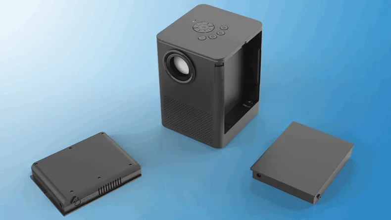
When selecting a PCB button, always match its height to the mechanical design of the device's case.
It's common to prototype with 2–3 different height options to find the perfect fit for both function and form.
Why height matters?
Clearance and alignment: If the button is too short or too tall, it may not align properly with the external enclosure, making it difficult to press or even damaging the PCB over time.
Tactile experience: Taller buttons can offer a more noticeable "click" or press feedback. In contrast, low-profile buttons might feel more modern or seamless, depending on the product aesthetic.
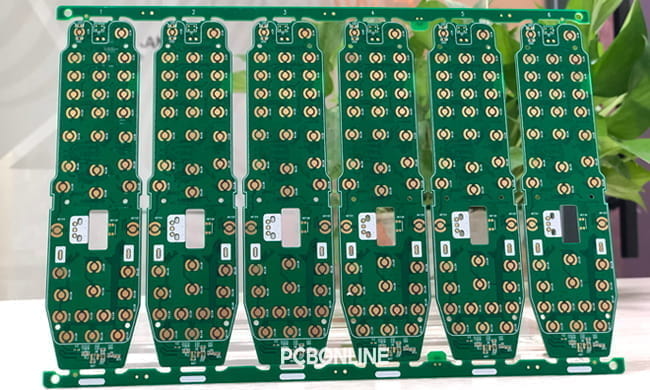
Designing PCB Button Pads
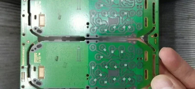
The pad layout on the PCB is where electrical contact happens, so it needs to be precise. Good pad design means better reliability, fewer soldering issues, and longer button life.
The common PCB button pad designs include a two-pad layout and circular/oval pad.
Two-pad layout: Most momentary buttons use two contacts that get bridged by a conductive element when pressed.
Circular or oval pads: These provide even force distribution and reliable contact.
When you design a PCB with any buttons, these tips can help your PCB design:
- Use support pads for SMD buttons. These pads don't carry electrical signals but add mechanical strength, especially useful for buttons that will be pressed often.
- Keep vias away from the contact area. Vias near the PCB button pads can create bumps or cause wear over time.
- Avoid routing traces directly under the pad area. This prevents interference and ensures the button presses cleanly.
- Use thicker copper layers or reinforce the PCB material around buttons to handle more stress.
- Avoid placing buttons near board edges unless supported by the enclosure or braced internally.
Because PCB buttons are subject to mechanical stress, especially in handheld devices or user-facing interfaces, reinforcing their mounting is critical.
If your product will undergo a lot of button presses, it's worth investing in a mechanically robust design from the start.
Surface Finishes for SMD Buttons
The surface finish on PCB button pads affects both electrical contact and durability.
Two of the most common finishes for PCB SMD buttons are carbon ink and hard gold plating.
Besides, selective gold plating is used for keyboard pads in high-end applications like medical keyboards.
Carbon ink
Carbon ink is a screen-printed conductive ink, typically used on lower-cost or high-cycle applications like remote controls or membrane keypads.
Pros:
- Inexpensive and easy to apply.
- Good wear resistance.
- Flexible in terms of pad shapes and sizes.
Cons:
- Higher contact resistance compared to metallic finishes.
- Less suitable for fine pitch or high-precision designs.
- Has no solderability and is only used for conductive contacts.
Hard gold plating
Also called electroplated gold, this finish involves electroplating a layer of hard gold (Ag + Co or Pd, 0.3μm-5μm) over nickel. It's often used in high-end and high-reliability applications.
If budget allows, hard gold is the premium choice for PCB button pads that require frequent wear. But for cost-sensitive products, carbon ink still provides solid performance for consumer-grade uses.
Pros:
- Extremely durable and resistant to wear.
- Very low contact resistance is great for signal integrity.
- Maintains performance over time and in harsh environments.
Cons:
- More expensive than other finishes.
- Requires tighter manufacturing controls.
- The weldability of hard gold is not good, so it's not used for button pads that need reflow soldering.
Selective gold plating
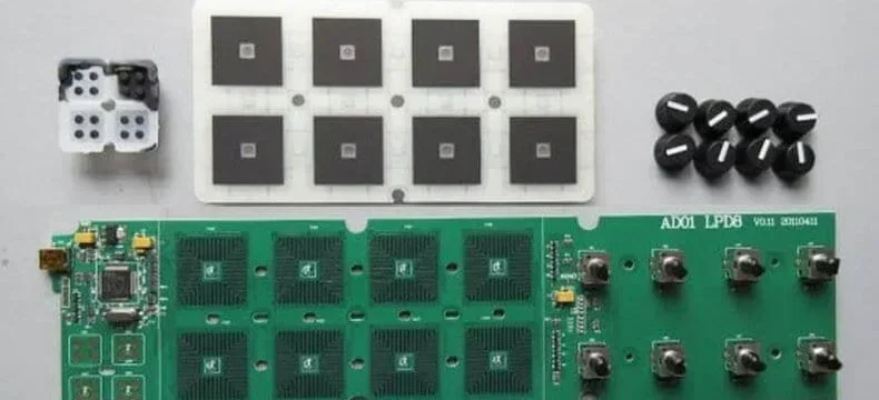
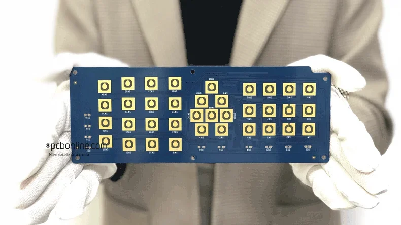
For high-precision applications where different button pads require different hardness, selective gold plating is used.
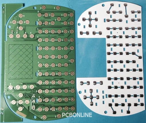
A typical example is the above medical button PCB, whose button pads will be installed with metal domes for presses in use. The PCB button pads that will be pressed frequently use hard gold plating as the surface finish and the ones that will be pressed much less use immersion gold.
ENIG (immersion gold)
The surface finish immersion gold involves depositing a thin layer of gold (0.05μm to 0.15 μm) over nickel. It provides excellent solderability and conductivity and is used for pads that have both soldering and button functions.
Pros:
- Superior solderability and small contact resistance.
- High-precision and suitable for fine-pitch designs.
- Maintains resistance against oxidation in humid environments.
Cons:
- Resistance again wear and impact is not very good.
- Not suitable for high-power buttons as the nickel layer of immersion gold may produce a "black nickel" problem under high current conditions.
Choosing the appropriate surface finish allows you to fine-tune your design based on budget, solderability, and wear expectations.
Special Case: PCB Power Buttons
Power buttons deserve special attention. While electrically they're just another momentary button, their role is central, turning the whole system on or off. These small design choices go a long way in ensuring a reliable and user-friendly power interface.
Key considerations in PCB power buttons are:
- Debouncing: Since button contacts can bounce, causing multiple triggers, debouncing is essential. This can be handled in hardware (using RC filters) or software (via firmware timing logic).
- Long-press logic: Many power buttons are designed to respond only to long presses to avoid accidental activation. Implementing this in firmware adds a layer of safety.
- Electrostatic discharge protection: Since the power button is often the first thing a user touches, it should be well shielded from static discharge.
- Placement and mechanical support: Power buttons are typically placed for easy access and should be reinforced to prevent board stress.
Don't overlook power buttons. They might be physically small, but they carry big responsibilities. Design them carefully with proper debouncing, mechanical support, and protection circuits to avoid issues down the line.
Turnkey Button PCB Manufacturer PCBONLINE from PCB to Enclosure Assembly
If you're looking for a professional PCB manufacturer that can handle buttons and any other details for your project, you can work with the turnkey PCB manufacturer PCBONLINE from R&D to one-stop PCBA manufacturing and box-build assembly.
Founded in 1999, PCBONLINE has two large advanced PCB manufacturing bases for button PCBs, one turnkey PCB assembly factory for button PCB assembly and box-build assembly, stable material supply chains and strategic cooperation with electronic component manufacturers, and long-term cooperation with the top 3 mold and enclosure manufacturers in China for jigs/fixtures, molds, and enclosures.
Besides, PCBONLINE has an R&D team and professional CAM engineers for project development and DFM (design for manufacturing).
PCBONLINE manufactures, assembles, and tests from button PCBs to box-builds as a source factory manufacturer under one roof, from prototypes to bulky production.
Complete PCB test equipment and capabilities for button PCB manufacturing and assembly, such as the AOI, flying probe test, ICT, X-ray, thermal shock, impedance, cross-section analysis, button strike life, four-terminal sensing, tension, bending, high-voltage, heat transfer, functional, thermal aging, and application simulation test.
Provides one-on-one free and professional DFM (design for manufacturing) for button PCB, PCBA, and box-build projects before and during prototyping/sampling to ensure the success of your project and seamless mass production.
PCBONLINE has rich experience in button PCB test and manufacturing fixture design, reflow/wave soldering temperature control, impedance control, and manufacturing procedure design.
High-quality button PCB manufacturing certified with ISO 9001:2015, ISO 14001:2015, IATF 16949:2016, RoHS, REACH, UL, and IPC-A-610 Class 2/3.
Besides button PCB tests, fabrication, components, and assembly, PCBONLINE provides value-added services such as conformal coating, waterproof encapsulation, IC programming, enclosures, and box-build assembly for your project.
By working with the one-stop PCBA manufacturer PCBONLINE, you don't need to find other providers for tests and enclosures, as all procedures, components, and enclosures can be provided by PCBONLINE. No matter what application your PCB will be used for, such as automotive, industrial control, medical, military, aerospace, communication, agriculture, etc, you can work with PCBONLINE. To reach out to the turnkey PCB manufacturer PCBONLINE, contact info@pcbonline.com.
Conclusion
PCB buttons might seem simple, but designing them well requires attention to mechanical, electrical, and ergonomic details. From selecting between SMD and PTH to matching button height to the enclosure, and choosing the right surface finish every decision contributes to performance and durability.
When all these details come together, you'll have PCB buttons that feel great, last long, and just work. To ensure the success of your button PCB/PCBA projects, work with the turnkey advanced PCB manufacturer PCBONLINE.
PCB assembly at PCBONLINE.pdf


