
In the field of electronic manufacturing, many people often confuse the concepts of SMD and SMT. This blog will help you understand what SMD and SMT are and how to choose in electronic manufacturing.
In this article:
Part 1. What services does PCB contract manufacturing provide? Part 2. What services does PCB contract manufacturing provide? Part 3. PCB contract manufacturing VS in-house processingYou may have heard the term PCB contract manufacturing somewhere, but your understanding of its meaning is vague. This blog will reveal what PCB contract manufacturing really is.
What is a PCB Contract Manufacturing?
PCB contract manufacturing is a service specifically provided to companies that need to outsource the production of circuit boards. PCB contract manufacturing has more advantages than in-house processing, such as cost control, delivery time, quality assurance, etc.
What services does PCB contract manufacturing provide?
R&D (optional)
The complete R&D service includes software and hardware R&D. The specific service terms include:
- Circuit diagram, PCB Layout design,
- BOM files to production process design
- Mold/fixture design, shell assembly design
- Test files and DFM process technical and non-technical problem solving (to ensure the smooth process of mass production and qualified quality of the final product)
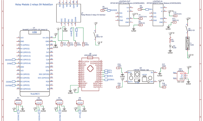
Integrated PCB Turnkey service
PCB contract manufacturers usually purchase components centrally based on BOM documents and then produce PCBs through internal production lines until they are finally assembled.
Then, according to customer needs, manufacturers seek specific suppliers to complete the mold/shell design and proofing adaptation, and once the sample is approved, mass production will be carried out directly.
Manufacturers provide a lot of hardware tests such as AOI, X-ray, flying probe, etc., and offer some value-added services such as functional tests and burn-in.
PCB contract manufacturing VS in-house processing
If you are a company decision-maker, how do you choose PCB contract manufacturing or in-house processing? We compare the differences between the two from different perspectives.
Manufacturing Flexibility
Designs may change or improve at any time, and ongoing projects may already be in the manufacturing stage. This is a less smooth process. The in-house processing mode is limited by fixed-configuration production lines, equipment and standard SOPs, and its adjustment range is relatively limited.
Contract manufacturing manufacturers can deal with this problem more flexibly. PCB contract manufacturers focus on two scales: proofing and batch production. The former is more economical and provides lower cost guarantees for companies that need to test samples continuously. Due to years of production experience, manufacturers are particularly good at adjusting production processes to optimize cost and quality issues
Cost Effect
Why is the total cost of internal processing for the same project much higher than outsourcing to a PCB factory?
The equipment and related quality inspection machines required for surface mount technology are a huge upfront investment, as is the cost of obtaining certification for manufacturing professional industry project PCBs. Secondly, the required components, SMD or single-chip microcomputers, and IC chips need to be purchased separately in small batches, which is costly. You also need to consider the employment costs of hiring employees. In addition, please consider a trial-and-error cost for internal processing. If you do not have mature project management experience, you may face many error problems in the proofing stage, which will increase unnecessary costs.
In contrast, contract manufacturers have more project orders from customers, some common components and centralized procurement, which greatly reduces the unit cost. In addition, after years of production experience, they have optimized the most economical production line configuration. Whether it is labor cost, material cost or equipment commissioning cost, it is usually lower than in-house processing.
Lead Time
Let's look at the differences between the two from different dimensions.
Feature |
Contract Manufacturing |
In-house Manufacturing |
Pre-set |
Slower (supplier selection, negotiation) |
Longer (equipment, plant, personnel, process establishment) |
Change Response |
Slower (communication, time difference) |
Faster (internal connection) |
Initial Build Time |
Fast |
Long |
Overall Period |
Depending on the order |
Usually longer |
Time Control |
Strong external dependency |
Strong internal control |
Comprehensive comparison
In-house processing:
- Expensive labor and equipment layout
- High unit price of components and high prototype cost
- Lack of extensive manufacturing experience, no mature project management and quality control to avoid risks
- May need to hire an expensive R&D team
- Other miscellaneous costs, certification fees, etc.
Comprehensive comparison
PCB contract manufacturing:
- Flexible supply chain
- Bulk centralized procurement of components, lower prototype costs
- Manufacturing experience accumulated from many orders, mature team and production history data can avoid potential risks
- Payment can be made in installments to reduce financial pressure
- Faster delivery and earlier market capture
In short, there is no best choice. This blog lists the differences in each aspect from the three aspects of economy, time and quality. The choice of production mode still depends on the specific demand for the product.
One-Stop HDI PCB Manufacturer and Its PCB Via Filing Capabilities
If you're looking for turnkey HDI electronics manufacturing services (EMS) from hardware development to PCBA fabrication and box-build assembly, you can work with the one-stop HDI PCBA manufacturer PCBONLINE.
Founded in 1999, PCBONLINE has R&D capabilities for HDI projects and EMS manufacturing capabilities, including via filling for stacked vias. It provides 4-to-64-layer HDI PCB fabrication, assembly, and PCBA box-build assembly. You can order various HDI PCBs from PCBONLINE, such as FR4, polyimide (flexible PCB), polyimide + FR4 (rigid-flex PCB), and PTFE/Rogers (high-frequency PCB).

3000m² of production capacity per day for HDI PCBs with builds of 1+N+1, 2+N+2, 3+N+3,4+N+4, and arbitrary interconnection in any layers.
PCBONLINE has hardware and software R&D capabilities for IoT applications requiring HDI design, including PCBA and enclosures.
We can manufacture complex PCBs with stacker vias, via-in-pad, microvias, inlay boards, heavy copper designs, and hybrid and fine structure lay-ups.
Besides HDI PCB fabrication, we have powerful capabilities in fine-pitch assembly for HDI PCB assembly.
We have rich R&D and manufacturing experience for HDI applications such as FPGA boards.
High-quality HDI PCB and PCBA manufacturing certified with ISO 9001:2015, IATF 16949, RoHS, REACH, UL, and IPC-A-610 Class 2/3.
Here'e the PCB via filing capabilities at PCBONLINEL:
- Micriavia filling with copper: laser via size 0.1-0.125mm, priority 0.1mm
- Finished hole size for via-in-pad filling with resin: 0.1-0.9mm (drill size 0.15-1.0mm), 0.3-0.55mm normal (drill size 0.4-0.65mm)
- Max aspect ratio for via-in-pad filling with resin PCB - 12: 1
- Min resin plugged PCB thickness: 0.2mm
- Max via-filling ith resin PCB thickness: 3.2mm
- Making different hole sizes with via filling in one board: Yes
- Via filling with copper/silver: Yes
If you need HDI PCBAs or any other PCBAs requiring via filling, please send your email to PCBONLINE at info@pcbonline.com. We will provide one-on-one engineering support to you.
Conclusion
Via filling is used for creating stacked vias in HDI PCB fabrication, BGA/CSP/QFN IC packaging, and filling PCB via-in-pad with resin during multilayer PCB fabrication. If you need one-stop electronics manufacturing for your HDI PCBA project, contact the one-stop advanced PCB manufacturer PCBONLINE for high-quality PCBA and box-build solutions tailored to your project's needs.
PCB fabrication at PCBONLINE.pdf


