
Electromagnetic interference (EMI) is a critical challenge in high-speed and high-frequency PCB design. Poor EMI shielding can lead to signal degradation, crosstalk, and regulatory compliance issues. Effective EMI shielding practices ensure signal integrity and electromagnetic compatibility (EMC), making it essential for engineers designing sensitive electronics.
This article provides an in-depth look into PCB EMI shielding techniques, best practices, and practical implementation methods. Besides, you can find a DFM (design for manufacturing) example for PCB EMI shielding by the one-stop high-frequency PCBA manufacturer PCBONLINE.
Understanding EMI in PCB Design
EMI originates from various sources, including external radiations, power fluctuations, and high-speed switching components. EMI issues in PCBs can manifest in two forms:
1. Radiated EMI: Emissions from PCB traces and components that can interfere with nearby electronics.
2. Conducted EMI: Noise propagating through power and ground planes, affecting the circuit performance.
To mitigate EMI, designers must implement shielding strategies that control and contain electromagnetic emissions.
PCB EMI Shielding Techniques
EMI shielding is a systematic work and should consider all perspectives in a system, including the ground plan, shielding layer, component placement, impedance control, filter capacitors, vias and routing, PCB material, and the shielding enclosure.
1. Ground plane and shielding layer
A well-designed PCB should have a continuous ground plane to provide a stable reference voltage and minimize EMI. The ground plane acts as a shield that absorbs and redirects EMI, preventing noise from spreading across the board.
- Use a continuous ground plane to create a low-impedance path for return currents.
- Employ multilayer PCBs with dedicated ground and power planes to reduce EMI.
- Avoid gaps in ground planes as they act as antennas for EMI.
2. Proper component placement
The positioning of components on a PCB directly impacts EMI performance. Proper component placement reduces crosstalk and enhances signal integrity by minimizing interference between analog and digital circuits.
- Place high-speed components near the center of the PCB to minimize edge emissions.
- Keep analog and digital circuits separate to reduce interference.
- Ensure power supply circuits are positioned away from sensitive signals.
3. Shielding cans and enclosures
Shielding cans and enclosures are critical for high-speed circuits and RF applications. These metallic covers prevent EMI from escaping and interfering with other nearby devices.
- Use metal shielding cans to enclose RF and high-speed components.
- Design PCB footprints to accommodate shielding covers if required.
- Ensure proper grounding of shields to avoid unwanted resonances.
4. Controlled impedance traces
Signal traces with uncontrolled impedance can cause signal reflections, leading to EMI issues. Controlled impedance design ensures that signals travel smoothly without significant loss or noise.
- Design signal traces with controlled impedance to prevent signal reflections.
- Use microstrip and stripline techniques in multi-layer PCBs.
- Maintain proper spacing between high-speed traces to reduce crosstalk.
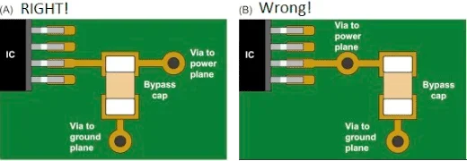
5. Filter and decoupling capacitors
Noise filtering is essential to maintaining clean power delivery and minimizing EMI. Decoupling capacitors act as local energy reservoirs to stabilize voltage and suppress high-frequency noise.
- Use bypass and decoupling capacitors near power pins of ICs.
- Select appropriate capacitor values to filter out high-frequency noise.
- Implement ferrite beads on power lines to suppress EMI.
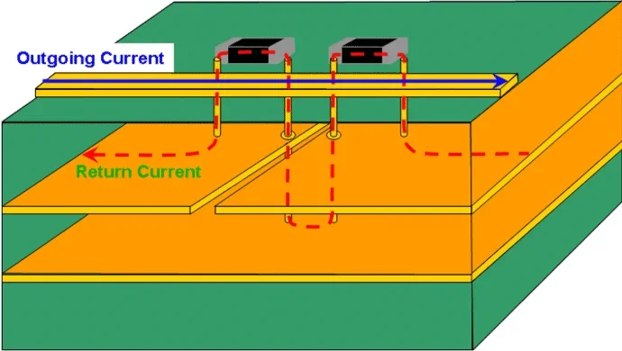
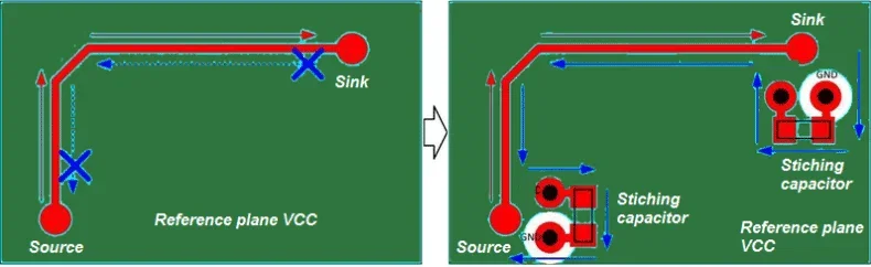
6. Via placement and routing strategies
Vias play a crucial role in EMI control by providing low-inductance paths for signals. However, poor via placement can cause impedance mismatches and excessive radiation.
- Use stitching vias near high-speed signals to improve grounding.
- Avoid excessive via transitions for critical traces to reduce impedance mismatches.
- Implement differential signal routing with tight coupling for better noise immunity.
7. PCB material selection
The choice of PCB material significantly affects EMI performance. Materials with stable dielectric properties and low loss help maintain signal integrity at high frequencies.
- Choose low-loss PCB materials (e.g., FR4, Rogers) for high-frequency designs.
- Use materials with stable dielectric properties to maintain signal integrity.
- Consider the use of conductive coatings to enhance shielding effectiveness.
8. Edge and aperture control
Uncontrolled PCB edges and openings in shielding structures can lead to EMI leakage, degrading the performance of sensitive circuits.
- Minimize gaps and apertures in metal shielding structures.
- Use PCB edge plating (via fencing) to reduce leakage of EMI signals.
- Maintain controlled trace terminations at board edges to avoid unintentional radiation.
Common EMI Mistakes to Avoid
Even with the best shielding techniques, certain design mistakes can lead to EMI issues. Avoiding these common pitfalls is crucial for achieving optimal EMC performance.
- Broken ground plane: A discontinuous ground plane forces high-frequency signals to take longer return paths, increasing loop area and radiation.
- High-speed signals near PCB edges: Placing high-speed signals too close to PCB edges can result in strong radiation, leading to unwanted emissions.
- Improperly grounded shielding Covers: If shielding enclosures are not properly grounded, they can act as antennas rather than suppressors, worsening EMI instead of mitigating it.
- Insufficient decoupling capacitors: Without proper decoupling capacitors, power fluctuations can introduce unwanted noise into sensitive circuits.
- Poor trace routing: Long, unshielded traces can act as antennas, picking up or radiating EMI. Keeping traces short and well-routed helps mitigate this issue.
- Overuse of signal-layer changes: Frequently switching layers with vias without proper grounding can introduce impedance mismatches and increase EMI emissions.
- Inadequate stitching vias: Without enough stitching vias, high-frequency signals may take unintended paths, increasing EMI susceptibility.
- Unterminated transmission lines: Leaving high-speed transmission lines improperly terminated can cause reflections, leading to EMI problems.
EMI Shielding Validation and Testing
To ensure effective EMI shielding, rigorous validation is necessary:
EMC compliance testing: Verify emissions and immunity standards (e.g., FCC, CE).
Near-field scanning: Detect hot spots and optimize shielding solutions.
Time-domain reflectometry (TDR): Measure impedance mismatches and refine PCB layout.
Antenna effect analysis: Check for unintended radiation sources within the PCB.
One-Stop High-Frequency PCBA Manufacturer with DFM for PCB Shielding
After you complete the EMI shielding validation, does it ensure the successful manufacturing for your project? Not yet. You will need a high-frequency PCB manufacturer PCBONLINE with rich DFM (design for manufacturing) experience to ensure no technical and non-technical issues for a seamless manufacturing process.

Founded in 1999, PCBONLINE has two large advanced PCB manufacturing bases, one PCB assembly factory, and an R&D team. For high-frequency PCB manufacturing, PCBONLINE is equipped with the plasma cleaning machine, laser drilling equipment, thermal shock equipment, and accurate etching line.
PCBONLINE provides free professional DFM before and during fabrication for your entire project, including PCB EMI shielding, and can offer improvement suggestions.
Complete high-frequency PCB manufacturing and testing, including mature etching technology, plasma treatment, trace width compensation with ±0.015mm accuracy, strict solder mask thickness control, and thermal shock at 288℃ for 10 seconds 1 to 3 times.
PCBONLINE has in-stock high-frequency laminates to reduce the PCB manufacturing lead time. Besides, for the best quality and performance of the PCB, our laminate storage time is within 45 days.
High-frequency PCBs made of any types, materials, and laminate brands are accessible, such as embedded antenna PCBs, PTFE, ceramic, PTFE/ceramic hybrid, Rogers, Taizhou Wangling, Taconic, etc.
No MOQ and no matter what quantity you want, we prioritize quality. The high-frequency PCBs and PCBAs are certified with SO 9001:2015, ISO14001:2015, IATF 16969, RoHS, REACH, UL, IPC-A-600 Class 2/3, and IPC-A-610 Class 2/3.
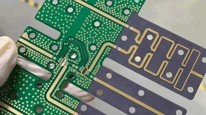
PCB EMI Shielding DFM: A Real Project IoT Scooter Motherboard
DFM for high-frequency PCB should not only check the Gerber and components to ensure no EMI technical mistakes, it should also foresee all details for manufacturing, assembly, and inspections to avoid interruptions and redesign when encountering the issue. PCBONLINE has rich DFM experience for high-frequency PCBs, and here's one real project example below.
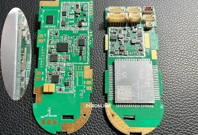
This is a motherboard project for IoT shared scooters. On the left side of the image, you can see the snap latches next to the components. These snap latches are designed to secure the metal shielding cover in place, protecting the components underneath from EMI.
Initially, our client designed the EMI shielding cover to be directly surface-mounted over the components, which can also prevent EMI.
However, during DFM, our engineer found that, in the PCB assembly process, the surface-mounted shielding cover would prevent AOI and X-ray inspection from operating to the beneath components. So we told our client it needs improving and suggested the snap patch design, allowing the AOI and X-ray inspection to those components, and fastening the metal enclosure after the AOI and X-ray inspection.
Besides, during DFM for this IoT scooter motherboard project, we also found three passive components in the PCB design have different footprints with their specifications in the BOM. Finally, this issue is fixed by revising the PCB pads and wiring.
What's more, we saved 15% component costs for our client, as we have strategic cooperation with the mainstream IoT communication module manufacturers.
PCBONLINE provides high-frequency PCB fabrication, PCB assembly, component sourcing, value-added services, and box-build assembly from prototypes to bulky production. If you need high-frequency PCBs with EMI shielding assistance, contact PCBONLINE by email at info@pcbonline.com to get a quote.
Conclusion
Effective PCB EMI shielding is crucial for high-frequency and high-speed applications. Implementing grounding techniques, shielding enclosures, proper trace routing, and using appropriate materials can significantly enhance EMC performance. Engineers must integrate these shielding strategies early in the design process to ensure compliance with EMI regulations and maintain reliable system performance.
By following the best practices, designers can achieve better EMI control, ensuring robust and interference-free PCB designs. For high-quality PCB manufacturing with excellent EMI shielding solutions, work with PCBONLINE to ensure reliable, low-noise, and high-performance circuit boards.
PCB Assembly from PCBONLINE.pdf


