
Grounding is essential in the design of any electrical system, including printed circuit boards (PCBs). Proper grounding ensures the PCB functions correctly, safely, and reliably. Without a PCB ground, problems like noise, interference, and even system failures can occur, especially in high-power or high-density PCB boards.
In this article, we'll discuss what PCB grounding is, different types of PCB grounds, the four common grounding mistakes to avoid, and best practices to keep your PCB designs running smoothly.
In this article:
Part 1: What is Ground in a Circuit? Part 2: Common Types of Grounding in PCB Design Part 3: The Four Deadly Grounding Sins to Avoid Part 4: Best Tips for Effective PCB Grounding Turnkey PCB Manufacturer PCBONLINE Ensuring Reliable GroundsWhat Is Ground in a Circuit?
A well-designed ground is crucial for ensuring clean signals, preventing thermal issues, and avoiding electromagnetic interference (EMI).
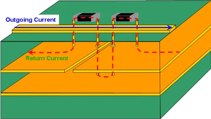
In a PCB, a ground plane is essentially a common return path for electric current. It serves as a reference point for all the voltages in the circuit, as the "zero" voltage level that helps everything stay on track.
There are two main roles that a ground plays in a circuit:
Reference point: It provides a universal "zero" point for measuring voltages across all components. Without a ground, components could be exposed to incorrect voltage levels, leading to performance issues or even damage.
Charge sink: It helps absorb any excess charge and prevents it from feeding back into other components, maintaining the system's stability.
Common Types of Grounding in PCB Design
Different PCB designs call for different grounding strategies. The right type of grounding depends on factors like circuit complexity, signal types, power requirements, and isolation needs.
Below are the most commonly used grounding approaches in PCB layouts:
- Power ground: This ground path is primarily used for handling return currents from power supplies, especially in DC systems. While it's essential for system stability, mixing power and signal grounds can introduce unwanted noise, so it's often best to keep them separate.
- Signal ground: Serving as the voltage reference for signal paths, this ground type is critical for maintaining signal integrity. For mixed-signal systems (analog + digital), isolating signal grounds is key to preventing cross-interference.
- Virtual ground: Found mostly in op-amp circuits, a virtual ground represents a midpoint voltage (like Vcc/2) rather than a direct connection to the actual ground plane. It's used as a local reference in specific configurations, such as voltage dividers or negative feedback loops.
- Floating ground: This refers to a ground that's electrically isolated from the main system or earth ground. It's common in isolated circuits like transformers, optical isolators, or battery-powered devices, where breaking the physical ground connection helps reduce ground loops or improve safety.
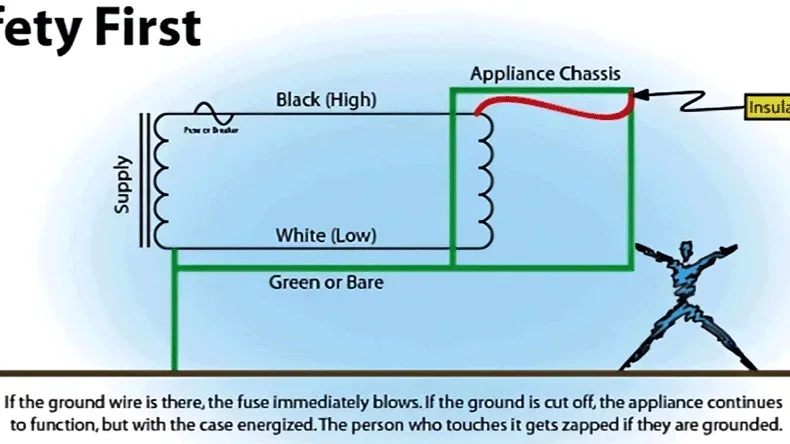
- Earth ground: Earth ground physically connects a circuit to the ground (literally the Earth). It's mainly used in high-voltage or safety-critical applications, providing a safe discharge path for fault currents or lightning surges.
- Shield ground: Also known as chassis GND. It is connected as a single point at the entry point of the cable or at the source side for EMI (electromagnetic interference) shielding of terminating cables and the enclosure.
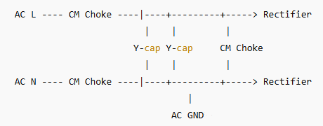
- AC ground: Also known as AC return or AC filtering ground in switch-mode power supplies (SMPS) and EMI management. The AC GND is for high-frequency noise filtering. It is connected to the bridge rectifier input side before galvanic isolation or the negative DC input trail after the bridge rectifier.
Here's an AC-DC SMPS input filter, for example:
Besides, you can check the table below for a clear understanding of the seven PCB ground types.
|
Type
|
Purpose
|
Critical applications
|
Tips
|
|
Signal GND
|
Signal integrity
|
ADCs, sensors
|
Keep analog/digital separate
|
|
Power GND
|
High-current return
|
Power supplies, motors
|
Use thick traces (> 50 mil)
|
|
Earth/Safety GND
|
Personal protection
|
AC-DC converters
|
Always comply with IEC 60364
|
|
Chassis/Shield GND
|
EMI mitigation
|
RF, shielded cables
|
Single-point connection
|
|
Virtual GND
|
Synthetic reference
|
Op-amp circuits
|
No actual current flow
|
|
Floating GND
|
Isolated system ground
|
DC-AC converters
|
Verify the potential difference
|
|
AC GND
|
High-frequency noise filtering
|
Switch-mode power supplies
|
Low impedance at high frequency
|
The Four Deadly Grounding Sins to Avoid
While grounding may seem straightforward, there are a few common mistakes that can cause big issues in your design. These four deadly grounding sins or mistakes should be avoided at all costs:
Ground loops
Ground loops happen when multiple current return paths are created due to differences in ground potential (ΔV = Iₜ × Rₗₒₒₚ). This leads to noise and instability, especially in high-speed circuits.
The symptoms of ground loops are 50/60Hz hum in audio systems and drifting DC offsets in sensor signals.
How to fix it: To prevent ground loops, use a star grounding approach where all ground connections meet at a single point. Keep your ground connections as short as possible and separate the power ground from signal grounds.
High-frequency impedance
High-frequency signals can face resistance and reflection issues if the return path isn't properly managed, leading to noise and signal degradation.
How to fix it: Use wide ground planes to minimize impedance, and place decoupling capacitors near the power pins of active components to filter out high-frequency noise.
Ground bounce
Ground bounce occurs when multiple components share the same ground path, causing fluctuations in the ground voltage due to inductance, leading to instability and noise.
A critical case of ground bounce is 200 mV ΔV between the MCU and ADC.
How to fix it: Use separate ground planes for high and low-voltage components, minimize the length of ground paths, and place ground vias close to sensitive components to provide dedicated return paths.
To prevent ground bounce, use < 5mm ground return paths for high-di/dt signals and low-inductance packages (e.g., QFN over DIP).
Plane resonance
Plane resonance is when large ground planes resonate at certain frequencies, causing unwanted oscillations and signal noise.
A typical scenario of plane resonance is a 237MHz resonance spike that appears during a Vector network analyzer (VNA) sweep. The spike corresponds to a λ/4 (quarter-wavelength) resonance in the 12cm plane.
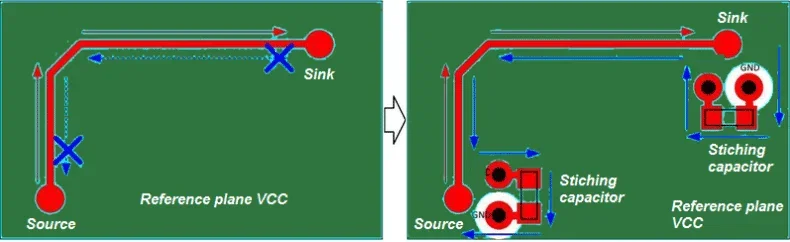
How to fix it: Use stitching vias (λ/10 spacing) to interconnect different layers of the ground plane, and consider adding absorptive materials like carbon-loaded EMI gaskets to dampen resonant frequencies.
Best Tips for Effective PCB Grounding
To ensure that your high-frequency PCB performs well, it's important to follow certain grounding techniques and best practices.
Here are some specific PCB grounding tips that have proven to work.
1. Use decoupling capacitors for power delivery optimization:
Place 100nF MLCC (0402) ≤3mm from IC power pins because 0402 footprints reduce ESL (equivalent series inductance).
Add bulk caps (10μF+) near power entry points (e.g., connectors/regulators) because they can handle low-frequency ripples.
2. Allocate ground pins of connectors:
Use 30% to 50% ground pins of high-speed interfaces like USB3.0 and HDMI. For example, for a USB 3.0 Type-A, use 4 ground pins out of the 9 total.
Stagger grounds between signal pins to improve return paths.
3. Reduce crosstalk for signal integrity
Minimize coupling with space parallel traces ≥3× trace width, which is critical for clock lines, differential lines, and high-speed singles.
4. Signal and GND allocation for a 4-layer PCB stackup
High-speed signals with controlled impedance in the Top Layer
Solid ground plane with minimal splits in Layer 2
Power plane with split voltages in Layer 3
Low-speed signals/chassis GND in Bottom Layer
Use 0.5mm (2oz) copper for power planes in a high-current PCB design.
5. Via optimization
Place ground vias near decoupling capacitors to reduce loop inductance (1 to 2 vias per capacitor).
Here is some general advice to help you design a reliable and noise-free PCB.
1. Use a dedicated ground plane
A dedicated ground plane is a copper layer that acts as the common reference for your PCB. It ensures that signals have a clear, stable path to return to. It also helps with signal routing and thermal management.
Tip: Keep the ground plane uniform to avoid voltage drops. Place the ground plane beneath the signal plane to reduce return path lengths and prevent noise from spreading.
2. Minimize ground loops
Ground loops are a major source of noise and interference. To avoid them:
Keep traces as short as possible.
Use separate ground planes for different sections of the PCB if necessary.
Avoid having multiple ground return paths that can create a loop.
3. Use bypass capacitors
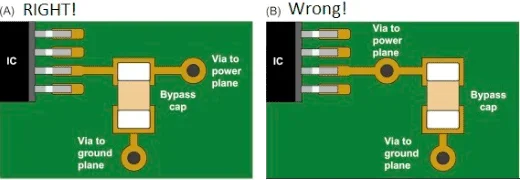
Bypass capacitors filter out noise and smooth out voltage fluctuations, especially on power rails. These capacitors are essential for preventing ground bounce.
Tip: Place bypass capacitors close to the power pins of active components to reduce noise and improve stability.
4. Minimize vias in the ground path
Excessive use of vias can add impedance to the ground path, leading to signal degradation. Always try to connect components directly to the ground plane.
Tip: Use fewer vias along the ground path to maintain signal integrity, especially in high-speed designs.
5. Use a single ground point (star grounding)
In complex designs, all ground connections must come together at a single point, called star grounding. This prevents interference and ensures a stable ground potential.
6. Plan for dynamic variance
When designing multi-board systems or systems with long cables, dynamic variance (i.e., differences between expected and actual performance) can affect the ground connection. To address this, use common-mode chokes and optical isolators to help mitigate any performance changes due to temperature or environmental factors.
7. Use surge protection
For high-voltage systems, surge and lightning protection are critical. Use power isolators, gas discharge tubes, and fuses to route excess energy away from the PCB and safely to ground.
8. Decoupling capacitors for a smooth power supply
Decoupling capacitors provide stable power to integrated circuits, smoothing out any voltage spikes or noise.
Tip: Distribute capacitors across the board, especially near power supply pins.
9. Understand the current flow
Understanding how the current flows through your circuit is essential for grounding. Plan your ground system with the signal and return paths in mind to prevent issues like ground bounce and instability.
Designing a power supply layout
Keep power components close together to minimize routing complexity and noise.
Shorter traces reduce inductance, which minimizes noise.
Use a solid, dedicated ground plane to improve both power and signal integrity and help with thermal dissipation.
Turnkey PCB Manufacturer PCBONLINE Ensuring Reliable Grounds
When you finish PCB design with careful grounding, to manufacture PCBs that meet the highest standards for performance and safety, you can work with the advanced PCB manufacturer PCBONLINE with R&D and EMS (electronic manufacturing service) capabilities.

Founded in 1999, PCBONLINE has two large advanced PCB manufacturing bases, one turnkey PCB assembly factory for PCB assembly and box-build assembly, stable material supply chains and strategic cooperation with electronic component manufacturers, and long-term cooperation with the top 3 mold and enclosure manufacturers in China for jigs/fixtures, molds, and enclosures.
Besides, PCBONLINE has an R&D team and professional CAM engineers for project development and DFM (design for manufacturing), which ensures the reliability of your PCB grounds.
PCBONLINE offers professional DFM (design for manufacturing), preventing any PCB grounding issues like noise, instability, and thermal problems.
The R&D team of PCBONLINE can complete or take part in the development of your project, including PCB grounding.
Provides one-on-one free and professional engineering support throughout your project, ensuring the premium PCB design, including PCB grounds, saving fabrication cost.
PCBONLINE manufactures, assembles, and tests from PCBs to box builds as an EMS manufacturer under one roof, from prototypes to massive production.
High-quality PCB and PCBA manufacturing certified with ISO 9001:2015, ISO 14001:2015, IATF 16949:2016, RoHS, REACH, UL, IPC-A-600 Class 2/3, and IPC-A-610 Class 2/3.
When your project goes to the massive production stage, PCBONLINE reduces the fees of prototyping, components of the prototypes, R&D, and offers free PCBA functional testing.
By working with the one-stop PCBA manufacturer PCBONLINE, you can ensure the reliability and safety of your PCB and box builds. No matter what application the PCB will be used for, such as automotive, communication, industrial, medical, military, aerospace, agriculture, etc, you can work with PCBONLINE. To get a quote for your project from the turnkey PCBA manufacturer PCBONLINE, contact info@pcbonline.com.
Conclusion
By following best practices, avoiding the four deadly grounding sins, and taking care to plan your grounding system thoughtfully, you'll ensure that your PCB works efficiently and without interference. Whether you're working on a high-speed design, a complex mixed-signal system, or a high-power board, you can work with the turnkey PCB manufacturer PCBONLINE for professional DFM, including checking grounding, and reliable PCB manufacturing and assembly.
PCB fabrication at PCBONLINE.pdf


