
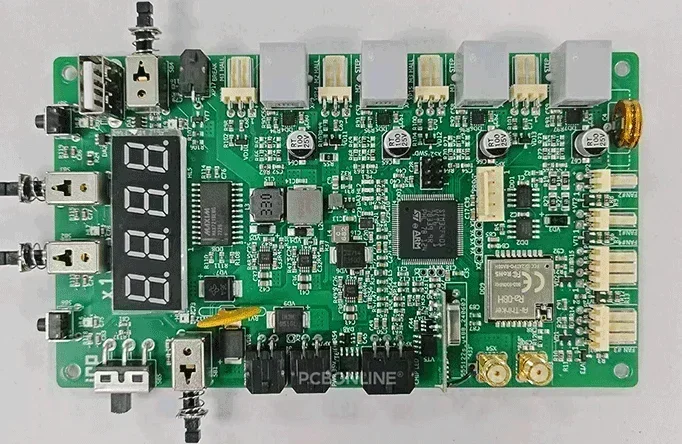
PCB soldering uses solder to attach the SMDs (surface-mount devices) to a PCB by melting the solder paste to create a strong solder joint. PCB assembly quality determines the terminal product's performance. Read the content below if you need PCB assembly for your project or have come with PCB soldering issues.
In this article:
Part 1. PCB Soldering Process Part 2. PCB Soldering Temperatures Part 3. PCB Soldering Issues and How to Ensure Success Part 4: High-Quality PCB Assembly Manufacturing Under One RoofPart 1. PCB Soldering Process
If your PCB projects are used for business or scientific purposes, you should use SMT (surface-mount technology) assembly for PCB soldering instead of hand soldering.
Compared with hand soldering, PCB SMT soldering is automatic, precise, and suitable for batch production. All the specs in PCB soldering, such as solder paste amount and soldering temperatures are controllable, so the PCBA quality is consistent and reliable.
What is the PCB soldering process at a PCB assembly factory? Easily understand the PCB soldering steps.
Step 1. Sending the board for solder paste printing
On a loader, the pieces of blank PCBs are placed on it. Each time, the loader sends a PCB with its tracker into the solder paste printing machine.
Note: Before solder past printing, we need to preheat the ceramic PCBs.
Step 2. Solder paste printing
![]()
In the solder paste printing machine, an SMT stencil is pre-set. The scraper presses a certain amount of solder paste to leap through the holes of the SMT stencil. The solder paste is then printed on the PCB pads corresponding to the SMD components to be placed.
Step 3. Solder paste inspection (SPI)
After solder paste printing, the board is sent by the guide through the SPI machine. The solder paste on PCB pads is scanned and compared with the reference specs range to ensure its size, thickness, and position are qualified for soldering.
Step 4. Placing SMD on PCB pads
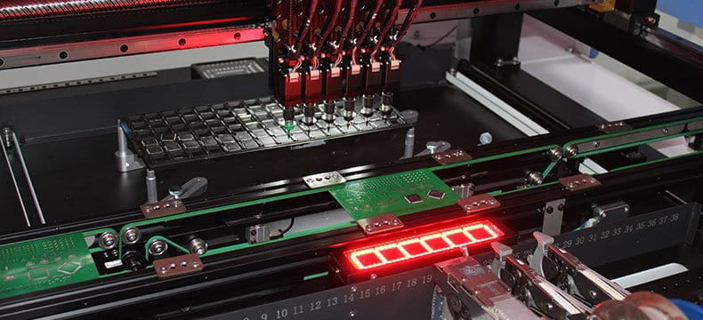
After SPI, the PCB board goes into the component surface-mount machine, where the robot arms pick SMDs from the feeders and place them one by one on the PCB.
Note: Now, if there's any BGA that has solder balls or an NTC (Negative Temperature Coefficiency) thermistor that needs dosing glue, there should be an X-ray inspection before the reflow soldering process.
Step 5. Reflow soldering
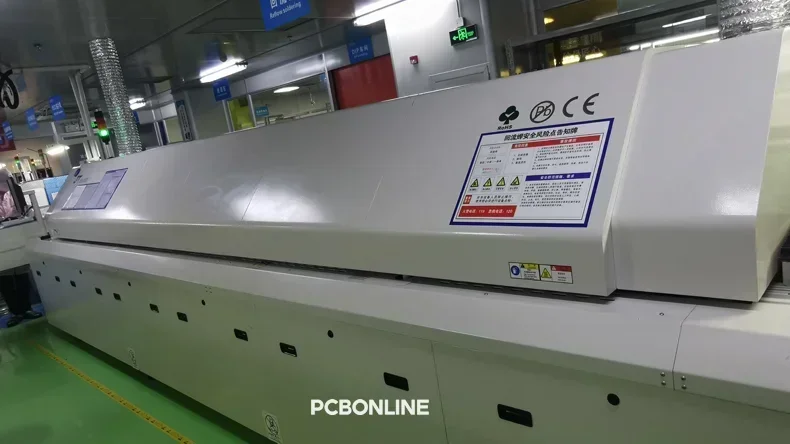
The board goes into the reflow soldering oven. In the oven, the solder melts at high temperatures. At the peak of reflow, the melting solder, PCB pad, and the SMD lead form an IMC (intermetallic compound) bond, which has strong electrical and mechanical strength. After the reflow soldering process, the board becomes a PCBA.
Nitrogen reflow soldering should ensure the oxygen content is below 4%.
Note: If the board also has a plated through-hole design, the PCBA is not finished yet. It needs PTH assembly on the other line.
Step 6. Automated optical inspection (AOI)
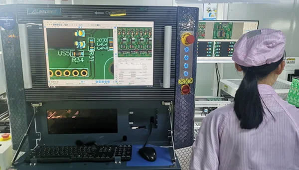
When the PCBA goes out from the reflow oven and naturally cools down, the PCBA is sent to pass the AOI machine which is also on the SMT line. There's a specialized AOI quality inspector for each SMT line to check the PCBA according to the machine markings and also visually inspect each board.
Note: If there's any surface issue with the PCBA, we send it for fix. After repair, the PCBA will be marked for identification and also separated from the good ones in the next PTH assembly and post-assembly stage and package.
Now you've learned the PCB soldering process. It is the details that determine the success of PCB soldering. Explore the PCB temperatures below.
Part 2. PCB Soldering Temperatures
The temperatures in the reflow soldering oven directly affect the PCB soldering quality. The PCBA manufacturers follow a reflow soldering profile to set up the temperatures of reflow.
Usually, the reflow soldering process has 4 stages and the PCB soldering temperatures are:
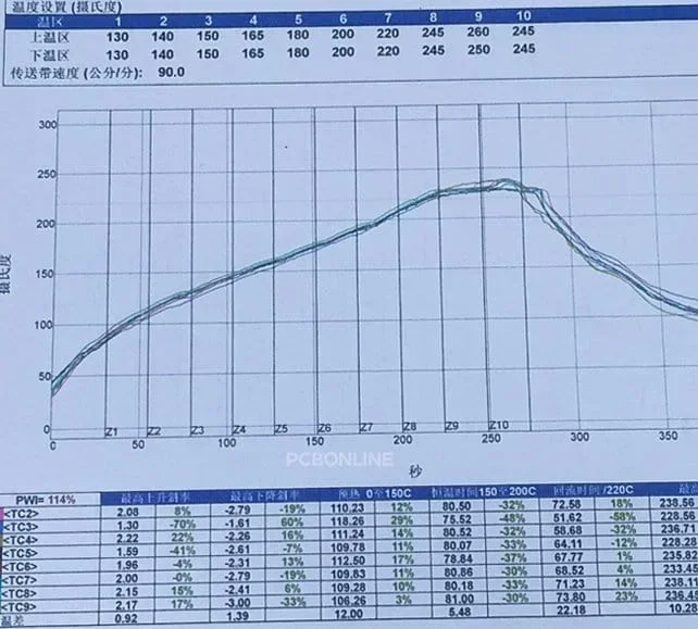
Preheat stage: 150°C to 190°C with a temperature increase slope rate of 0.75℃/sec to 2℃/sec. The preheat stage lasts about 60s to 120s.
Soak stage: Should reach about 217°C with a temperature increase slope rate of 0.5℃/sec to 1℃/sec. The preheat stage lasts about 60s to 120s.
Reflow soldering stage: should reach 240°C to 248°C. The reflow stage lasts about 40s to 70s and within it, the peak lasts 10s to 30s.
Cooling stage: the temperatures go down from the peak to 75°C. The cooling stage lasts 10s to 30s.
It should be noted that thick-copper PCBs and ceramic PCBs dissipate heat much more quickly than FR4 PCBs, so the PCB soldering temperatures should be 20°C higher, and the PCB should go through the oven more quickly.
Part 3. PCB Soldering Issues and How to Ensure Success
A poor PCB soldering process can lead to many PCB soldering issues, including cold welding, non-welding (non-wetting), tombstoning, solder bridges, solder voids, and solder balling.
Below, we introduce these PCB soldering issues and our tips to ensure PCB soldering success.
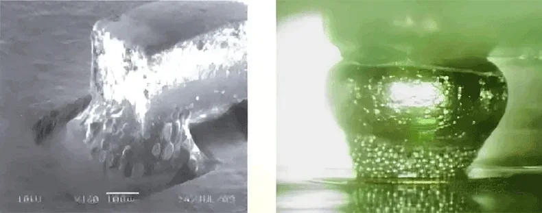
Cold welding: There is no tin strip formed at the tinning interface of the SMD component, and the solder joint usually has a rough, dull, granular surface like tin powder (i.e., poor tinning).
Too long constant temperature time, too low reflow temperatures, too short reflow time, tinning solderability problems, etc. will cause cold welding.
We will adjust your design to improve it until the sample yields satisfying results. So you don't need to worry about quality issues by working with the OEM PCB manufacturer PCBONLINE.
The common solution is increasing the reflow soldering temperatures and reflow soak and peak time.
Non-welding (non-wetting): There is only a small amount of solder at the solder joint, resulting in poor contact and intermittent electrical testing.
Non-wetting is caused by not cleaning the PCB pad on the surface of SMD or printing too little flux on the PCB pad.
The solution is strengthening the PCB cleaning process after plating during PCB fabrication, using high-quality solder paste, and improving the SMT stencil design to leap enough solder paste on the PCB pads.
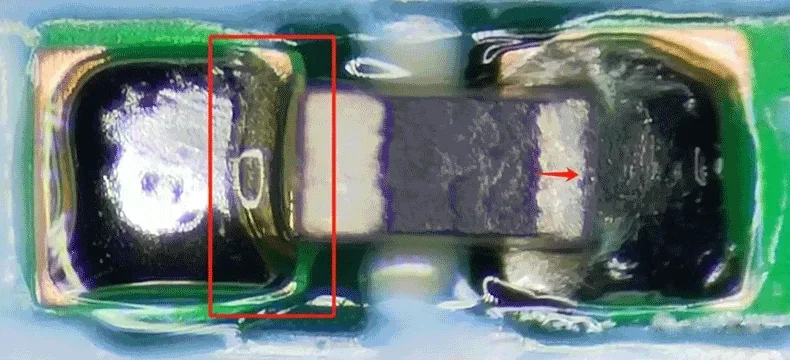
Tombstoning (Manhattan effect): An end of the SMD component is partially or completely lifted from the PCB pad.
Uneven solder paste on the PCB pad, inaccurate component placement, and uneven heating during reflow can cause tombstoning.
The solution is using an automatic SMT machine rather than hand soldering, avoiding the component orientation to be in parallel with the reflow conveyor, and optimizing the PCB pad design. Besides, SPI is a must to ensure the solder paste on PCB pads is qualified for soldering.
![]()
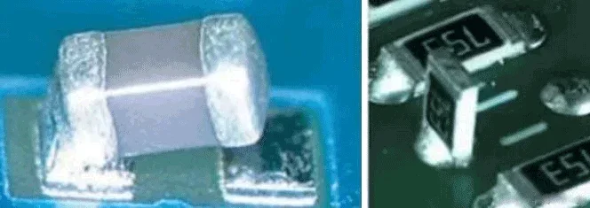
Solder bridges: excessive solder outside the intended solder joint connects two adjacent solder conductive elements. It can cause short circuits.
Excessive solder paste on PCB pads, inaccurate component placement, and too close adjacent PCB pads will cause solder bridges.
The solutions is using an automatic SMT machine rather than hand soldering, SPI inspection, PCB design optimization, and improving the SMT stencil design to prevent excessive solder paste on the PCB pads.
![]()
Solder voids: Empty spaces or air pockets within the solder joint.
The causes of this issue include uneven solder paste printing and trapped flux or gases during reflow.
The solution is using fully automatic SMT assembly and increasing the reflow soldering temperatures and soak time.
![]()
Solder balling: Unintended solder balls on the PCBA surface. It can cause short circuits.
Excessive solder paste on PCB pads and rapid cooling can cause this issue.
The solution is also controlling the amount of solder paste with a proper SMT stencil design. Besides, avoiding rapid cooling and ensuring a controlled reflow process.
Part 4: High-Quality PCB Assembly Manufacturing Under One Roof
For high-quality PCBA manufacturing without PCB soldering issues and lead to success, you can work with the one-stop PCB assembly manufacturer PCBONLINE. It provides free DFM for hassle-free manufacturing.
Founded in 1999, PCBONLINE has two large advanced PCB manufacturing bases, one PCB assembly factory, stable supply chains, and an R&D team.
Before and during PCBA prototyping, PCBONLINE offers free DFM to ensure PCB soldering success, including Gerber and BOM checks, manufacturing and testing process design, selecting alternative components with the same functions and certifications to reduce fabrication costs, and solving issues throughout the prototype and product sampling stage.
PCBONLINE has rich experience in SMT stencil design to ensure the proper amount of solder paste on pads for PCB soldering.
Fully automatic SMT assembly lines for PCB soldering, including the 3D SPI, nitrogen reflow soldering, and 3D AOI.
High-quality PCB, PCBA, and box-build manufacturing certified with ISO 9001:2015, ISO 14001:2015, IATF 16949:2016, RoHS, REACH, UL, and IPC-A-610 Class 2/3.
Comprehensive testing and value-added services in the post-assembly stage to ensure the success of your PCBA project, including PCBA functional testing, conformal coating, IC burn-in programming, thermal aging, final product box-build assembly, and application simulation testing.
Whether you are a small to middle-scale terminal company, solution company, business maker, or research institute, you can have your PCBA project manufactured by PCBONLINE. To get a quote for your project with medical and military-grade PCB soldering quality, email info@pcbonline.com.
Conclusion
This blog covers all aspects of PCB soldering. For one-stop PCB manufacturing and high-quality PCB soldering, work with the OEM PCB manufacturer PCBONLINE.
PCB assembly at PCBONLINE.pdf


