
PCB (printed circuit board) tests are a systematic work throughout the PCB design, fabrication, assembly, and box-build assembly process. What files do you need to provide for your PCB manufacturer for testing from PCB fabrication, PCB assembly, to enclosure assembly until your final electronic devices are finished? And what PCB tests will your turnkey PCB manufacturer PCBONLINE provide?
In this article, the turnkey PCB manufacturer PCBONLINE introduces PCB tests comprehensively, including testing files and PCB tests following the electronic manufacturing process order.
In this article:
Part 1. What are the PCB Test Files? Part 2. PCB Tests During PCB Manufacturing One by One Part 3. Turnkey PCB Manufacturer PCBONLINE with Comprehensive PCB TestsWhat are the PCB Test Files?
When you design a PCB, what test files will you create to provide for the PCB manufacturer for PCB testing? The test files of AOI (automated optical inspection), X-ray, ICT (in-circuit test), and and their design/guidelines are provided by the PCB manufacturer. However, you still need to provide the below files for the turnkey PCB manufacturer PCBONLINE for PCB testing.
- Netlist: Generate the netlist from a PCB design tool. A netlist specifies the PCB's electrical connections so the PCB manufacturer can compare them with the PCB electrical testing results. It is in the IPC-D-356 or IPC356 format.
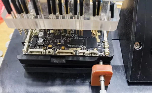
- Test point file: If your PCB needs an in-circuit test, design the holes with pads for the ICT and generate the test point file from the PCB design tool. It enables the PCB manufacturer to design the ICT fixture according to the test points' position (XY).
- Test requirements for other PCB tests: If your PCB requires the high-voltage test, impedance control test, four-terminal sensing test, etc, please tell PCBONLINE your PCB's testing requirements.
Besides the above PCB test files, send the below necessary files for PCB fabrication and assembly, which are associated with PCB tests.
Gerber: Generate the Gerber from the schematic for the PCB manufacturer to understand your PCB requirements. The Gerber compressed package includes the graphics for each layer of the PCB and a drill file specifying the positions and sizes of the PCB holes.
BOM: Generate the BOM (bill of material) from the PCB design tool. If your project is simple, you can create an Excel to make the BOM. After creating the BOM, carefully check it to ensure the components' spec match their PCB footprints. To add more details, You can add the component manufacturer and the manufacturer's component model to the BOM. You can also generate the 3D image of the assembly for the PCBA manufacturer to match.
Enclosure design: If your PCB requires enclosure assembly, send the enclosure graphics or pictures to the turnkey PCB manufacturer PCBONLINE. PCBONLINE has long-term cooperation with the top 3 mold/enclosure manufacturers in China and will have the enclosure manufactured. After assembling the enclosure onto the PCBA, there's the application simulation test.
PCB Tests During PCB Manufacturing One by One
After you send the Gerber, necessary PCB test files, BOM, and enclosure design to the turnkey PCB manufacturer PCBONLINE, the engineers at PCBONLINE check your documents, do DM (design for manufacturing), and solve technical issues, including PCB test procedures, AOI rules, flying probe test program and tolerance file, ICT fixture layout, test vector file, and the mold design.
The PCB tests in the PCB manufacturing process are below.
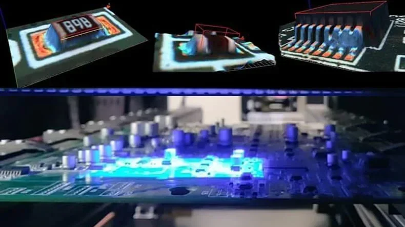
AOI in PCB fabrication: During PCB manufacturing, each copper layer is etched to be the circuit graphic. When a PCB layer is completed, there's the AOI to ensure it matches the circuit graphics in the Gerber.
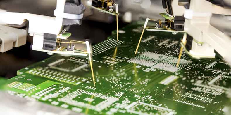
Flying probe test: A flying probe test is an electrical test using the four probes to touch the PCB pads and holes to ensure no open or short circuit in the PCB. It doesn't need a fixture. If your PCB boards are in a small quantity, or there are no test points, especially HDI PCBs, the flying probe test is available.
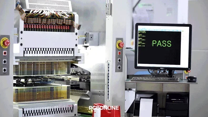
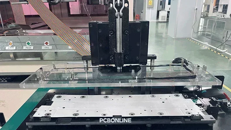
In-circuit test (ICT): An ICT is also an electrical test to ensure no open or short circuit in the PCB. It also tests the resistors and capacitors' specs. It requires a fixture, which is designed by your PCB manufacturer. If your PCB boards are in large quantity, the ICT is available, and the fixture can be used all the way throughout your project from prototypes to bulky production.
Note:
Both the flying probe test and ICT are an electrical test after PCB fabrication to ensure no open or short circuits. Usually, a flying probe test or an ICT is enough for a PCB E-test.
X-ray inspection in embedded or HDI PCB fabrication: HDI PCBs have staggered or stacked vias. After lamination, there's an X-ray inspection to ensure the hole copper quality in the HDI PCB. Besides, if a multilayer PCB has any embedded component or cavity, it is also inspected with X-ray after PCB lamination.
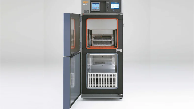
Thermal shock testing for high-frequency PCB: After high-frequency PCB fabrication, there's a thermal shock test to ensure the hole walls don't separate under temperature changes. It is at 288℃ for 10 seconds, from 1 to 3 times.
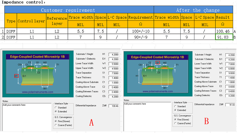
Impedance test for HDI PCB and high-frequency PCB: After HDI or high-frequency PCB manufacturing, there's an impedance test using an impedance tester to ensure the impedance control matches the design requirements. Usually, it is 50Ω.
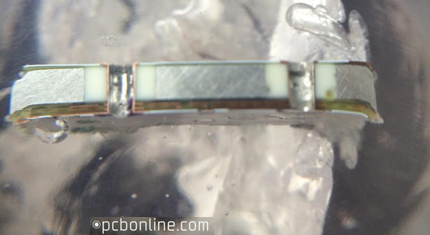
Metallographic test for copper thickness: After fabrication of double-sided aluminum PCB, multilayer copper-core PCB, or flexible PCB, there can be a metallographic test that cuts the PCB to analyze its cross-section.
Button strike test for PCB buttons: If your PCB has any button, after PCB fabrication, there can be a button strike test to ensure the buttons can be pushed thousands of times meeting the expected requirements.
Four-terminal sensing for high-end applications: For advanced PCBs used for military, aerospace, automotive, and medical applications, reliability is vital. Four-terminal sensing, also called the Kelvin test, accurately tests the micro resistance of the PCB's circuit lines and contacts. It ensures the PCB's copper is evenly etched and plated.
Tension and bending tests for flexible PCBs: If a flexible PCB needs to stretch and bend in the device working, there are a tension test and bending test using the below two testers to ensure the flex PCB meets the expected withstand effect.
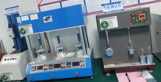
High-voltage and heat transfer tests: If your PCB is used for high-power applications, its PCB tests should include the high-voltage and heat transfer tests. These two tests are quite simple — using a dielectric strength tester to let the PCB work at high voltages like 220V, 500V, etc, and using a thermometric indicator to check the temperature of the PCB immediately after working at the high voltage.
Above are the PCB tests in the PCB fabrication process. During PCB assembly, there are also PCB assembly tests, including solder paste inspection, AOI, and X-ray inspection. After PCB assembly, there are PCBA tests, including the functional test and thermal aging. After box-build assembly, there's the application simulation test.
Turnkey PCB Manufacturer PCBONLINE with Comprehensive PCB Tests
If you're looking for a professional PCB manufacturer that can handle all the tests and electronics manufacturing for your project, you can work with the turnkey PCB manufacturer PCBONLINE from R&D to one-stop PCB manufacturing and box-build assembly.
Founded in 1999, PCBONLINE has two large advanced PCB manufacturing bases for waterproof PCBs, one turnkey PCB assembly factory for waterproof PCB assembly and box-build assembly, stable material supply chains and strategic cooperation with electronic component manufacturers, and long-term cooperation with the top 3 mold and enclosure manufacturers in China for jigs/fixtures, molds, and enclosures.
Besides, PCBONLINE has an R&D team and professional CAM engineers for project development and DFM (design for manufacturing), including all aspects of PCB tests.
PCBONLINE manufactures, assembles, and tests from PCBs to box-builds as a source factory manufacturer under one roof, from prototypes to bulky production.
Complete PCB test equipment and capabilities for PCB manufacturing and assembly, such as the AOI, flying probe test, ICT, X-ray, thermal shock, impedance, cross-section analysis, button strike, four-terminal sensing, tension, bending, high-voltage, heat transfer, functional, thermal aging, and application simulation test.
Provides one-on-one free and professional DFM (design for manufacturing) for PCB, PCBA, and box-build projects before and during prototyping/sampling to ensure the success of your project and seamless mass production.
PCBONLINE has rich experience in PCB test and manufacturing fixture design, reflow/wave soldering temperature control, impedance control, and test and manufacturing procedure design.
High-quality PCB manufacturing certified with ISO 9001:2015, ISO 14001:2015, IATF 16949:2016, RoHS, REACH, UL, and IPC-A-610 Class 2/3.
PCBONLINE can design the test points for your PCB and offer improvement suggestions for your PCB design if there's any problem.
Besides PCB tests, fabrication, components, and assembly, PCBONLINE provides value-added services such as conformal coating, waterproof encapsulation, IC programming, enclosures, and box-build assembly for your PCB project.
By working with the one-stop PCBA manufacturer PCBONLINE, you don't need to find other providers for tests and inspections. No matter what application your PCB will be used for, such as automotive, industrial control, medical, military, aerospace, communication, agriculture, etc, you can work with PCBONLINE. To reach out to the turnkey PCB manufacturer PCBONLINE, contact info@pcbonline.com.
Conclusion
This blog introduces what PCB test files are needed and the PCB tests one by one. PCB tests are not independent of electronics manufacturing but are contained in the PCB and PCBA manufacturing process. To ensure the success of your PCB/PCBA projects, work with the turnkey advanced PCB manufacturer PCBONLINE.
PCB fabrication at PCBONLINE.pdf


