
Via filling is a fabrication step in BGA packaging and multilayer PCB fabrication, especially for HDI PCBs with stacked vias. This blog gives a comprehensive introduction to via filling, including the types of via filling, how to fill vias in a PCB, and the PCB via filling fabrication capabilities at the one-stop PCBA manufacturer PCBONLINE.
In this article:
Part 1. What is Via Filling Part 2. Types of Via Filling Part 3. How to Fill Vias in a PCB Part 4. One-Stop HDI PCB Manufacturer and Its PCB Via Filing CapabilitiesWhat is Via Filling
Via filling means filling the PCB via/hole with resin or electroplating after the PCB hole is plated with copper during PCB fabrication. In HDI PCBs, microvias need the via filling process.
The aim of PCB via filling is to improve the PCB via's mechanical strength and flatness.
With the flat surface, the upcoming step after via filing, such as stacking the upper via and PCB layer, or soldering components, can proceed smoothly without potential risks. Besides, if the PCB via is filled with copper or silver, via filling increases electrical and thermal conductivity.
Via filling is not applied for all PCBs, but only in these scenarios:
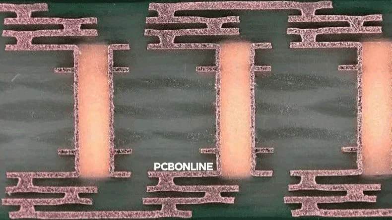
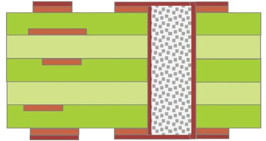
Creating stacked vias
A stacked via consists of multiple layers of microvias created by laminating the outer layers, known as serial lamination.
Before laminating, the microvias have been pre-drilled and plated on each outer layer.
When an outer layer is laminated on the top and at the bottom of the PCB core layers, its microvias in the current outer layer are filled with copper.
Thanks to via filling, the upper structure of the stacked via can be made successfully.
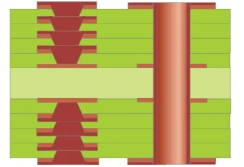
Why do stacked vias need filling?
One reason is increasing mechanical strength. In a multi-layer stacked via structure, the microvias closer to the inner layers may become shallow, or their walls may not be strong enough due to the large layer number of microvias. Via filling can enhance the mechanical strength of the stacked via structure and avoid damage to the hole walls.
The other reason is flattening the surface. When the stacked via overlaps with the PCB component soldering area, it is important to flatten the end of the stacked via to ensure soldering quality and avoid solder penetration into the via. Via filling flattens the surface of the stacked via to the PCB surface.
Filling resin into vias in-pad
A via-in-pad is a through-hole or blind hole drilled in the PCB pad. It not only solders a PCB SMD component but also dissipates heat quickly.
The via-in-pad requires via filling with resin in the PCB fabrication process to prevent the solder from flowing into it during reflow soldering.
Besides, via filling with resin increases the mechanical strength of the pad and the hole wall.
What's more, for high-speed or RF PCBs, filling the via-in-pad with resin can reduce signal reflection and improve signal integrity.
Packaging BGA and CSP
In the IC packaging companies, the fabrication process of BGA, CSP, and QFN requires via filling. BGA, CSP, and QFN are high-density IC packages, and inside them, there are minor holes from the chip to the bottom of the packages. These minor holes are needed via filling to ensure the reliability of the package itself and the mechanical strength of the solder ball connection.
Besides, via filling prevents the solder from flowing into the minor holes of the IC package during BGA PCB assembly.
In addition, vias in high-power IC BGA packages are filled with copper, which helps thermal management.
Types of Via Filling
Will via filling with resin affect the electric conductivity of the PCB vias? No. If the microvias are filled with resin, it only fills the via without affecting the electric connection.
The different filling materials lead to different types of via filling.
Via filling with resin
Stacked vias in HDI PCBs and via-in-pads in multilayer PCBs require via filling with resin.
Via filling with resin or resin plugging is the most affordable way for PCB via filling.
The resin for via filling is epoxy resin or polyimide resin. It has good insulation, high-temperature resistance, and mechanical strength.
Via filling with resin is using the proxy resin to fill the PCB via following copper plating, and then flattening the via surface by removing the extra resin.
It only fills the gaps in the minor via to increase the mechanical strength of the via and soldering flatness.
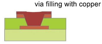
Via filling with copper
Stacked vias in HDI PCB and BGA/CSP/QFN IC packaging require via filling with copper.
Copper is the most common material for via filling for HDI PCBs.
In creating the stacked vias during HDI PCB manufacturing, each layer's microvias can be filled with copper before laminating the next outer layer with microvias.
Filling the microvia with copper is necessary before laminating the next outer layer to the PCB core. It flattens the surface, and strengthens the mechanical strength of the microvia, improving the thermal conductivity and connectivity of the HDI PCB.
Via filling with silver
Silver is rarely used for via filling because it costs more than copper. However, if the HDI PCB is used for high-speed/radio-frequency applications and requires low contact resistance, its microvias can be filled with silver, as silver has the best conductivity.
Though silver is rarely used for via filling, it is the only option for circuit connectivity for wiring and plating through holes for PCBs that require low temperatures for SMT reflow soldering. For example, all the wires and holes in the transparent flexible PCB made of PET (polyester) materials are silver.
How to Fill Vias in a PCB
The via filling process using resin or copper/silver is different. Resin is plugged in to fill the hole, while copper and silver are plated to fill the hole.
Below is how to fill the vias in a PCB.
Filling PCB vias with resin plugging
In HDI PCB with stacked vias or other multi-layer boards with via-in-pad, vias can be filled with resin.
Before filling the via with resin, copper has already been electroplated in the hole to achieve an electrical connection.
Then the remaining space in the hole will be filled with epoxy resin or polyimide resin.
After filling the resin, it is grinding and removing excess resin to ensure that the surface of the hole is flat. The resin filling only exists inside the hole.
Next, the resin is baked to consolidate tightly into the hole.Filling PCB stacked vias with copper/silver
In HDI PCB fabrication, the microvia is pre-drilled and plated with copper before laminating.
During serial laminating, each layer of microvia is plated with copper to fill the hole and grinding to flatten the surface before the next layer is laminated onto it.
After serial lamination, the HDI PCB is silk screen printed with solder masks to complete the HDI PCB fabrication.
One-Stop HDI PCB Manufacturer and Its PCB Via Filing Capabilities
If you're looking for turnkey HDI electronics manufacturing services (EMS) from hardware development to PCBA fabrication and box-build assembly, you can work with the one-stop HDI PCBA manufacturer PCBONLINE.
Founded in 1999, PCBONLINE has R&D capabilities for HDI projects and EMS manufacturing capabilities, including via filling for stacked vias. It provides 4-to-64-layer HDI PCB fabrication, assembly, and PCBA box-build assembly. You can order various HDI PCBs from PCBONLINE, such as FR4, polyimide (flexible PCB), polyimide + FR4 (rigid-flex PCB), and PTFE/Rogers (high-frequency PCB).

3000m² of production capacity per day for HDI PCBs with builds of 1+N+1, 2+N+2, 3+N+3,4+N+4, and arbitrary interconnection in any layers.
PCBONLINE has hardware and software R&D capabilities for IoT applications requiring HDI design, including PCBA and enclosures.
We can manufacture complex PCBs with stacker vias, via-in-pad, microvias, inlay boards, heavy copper designs, and hybrid and fine structure lay-ups.
Besides HDI PCB fabrication, we have powerful capabilities in fine-pitch assembly for HDI PCB assembly.
We have rich R&D and manufacturing experience for HDI applications such as FPGA boards.
High-quality HDI PCB and PCBA manufacturing certified with ISO 9001:2015, IATF 16949, RoHS, REACH, UL, and IPC-A-610 Class 2/3.
Here'e the PCB via filing capabilities at PCBONLINEL:
- Micriavia filling with copper: laser via size 0.1-0.125mm, priority 0.1mm
- Finished hole size for via-in-pad filling with resin: 0.1-0.9mm (drill size 0.15-1.0mm), 0.3-0.55mm normal (drill size 0.4-0.65mm)
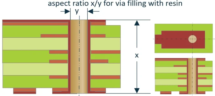
- Max aspect ratio for via-in-pad filling with resin PCB - 12: 1
- Min resin plugged PCB thickness: 0.2mm
- Max via-filling ith resin PCB thickness: 3.2mm
- Making different hole sizes with via filling in one board: Yes
- Via filling with copper/silver: Yes
If you need HDI PCBAs or any other PCBAs requiring via filling, please send your email to PCBONLINE at info@pcbonline.com. We will provide one-on-one engineering support to you.
Conclusion
Via filling is used for creating stacked vias in HDI PCB fabrication, BGA/CSP/QFN IC packaging, and filling PCB via-in-pad with resin during multilayer PCB fabrication. If you need one-stop electronics manufacturing for your HDI PCBA project, contact the one-stop advanced PCB manufacturer PCBONLINE for high-quality PCBA and box-build solutions tailored to your project's needs.
PCB fabrication at PCBONLINE.pdf


