
When you design a PCB (printed circuit board) with any small-pitch components, such as BGAs and FPGAs, you may find it takes too much space for regular routing around the pad. An efficient way is to place the via in the pad. In this blog, you will learn about PCB via in pad comprehensively, including what it is, its requirements, and how to create a via in pad in PCBs.
In this article:
Part 1. What is PCB Via in Pad? Part 2. Situation to Use Via-in-Pad in Your PCB Part 3. How to Make PCB Via-in-Pads Turnkey Advanced and HDI PCB Manufacturer with Via-in-Pads CapabilitiesWhat is PCB Via in Pad?
A via-in-pad refers to a through-hole or blind hole drilled in the PCB pad. The hole in the pad is filled with resin and then copper-capped to form a seamless connection to the pad. It can increase wiring density and improve signal integrity.
If your PCB is a regular multilayer PCB, the hole in the via-in-pad is a through hole. If it is an HDI PCB or with an ultra fine-pitch BGA (center-to-center distance between adjacent solder balls being 0.5mm and below), the hole in the via-in-pad is a blind via.
Note: Since there are no pins to be soldered in the middle of the IC, there is no need to consider tin leakage or cold soldering for the via in the IC heat dissipation pad. However, the via diameter should be as small as possible. What's more, a through hole is still prohibited from placing in the pad with electrical networks (such as GND net), but a blind via can be placed in the pad.
How does a via-in-pad work? During PCB assembly, an IC is surface mounted to solder on the PCB via-in-pad, and its ball connects the hole to dissipate heat quickly.
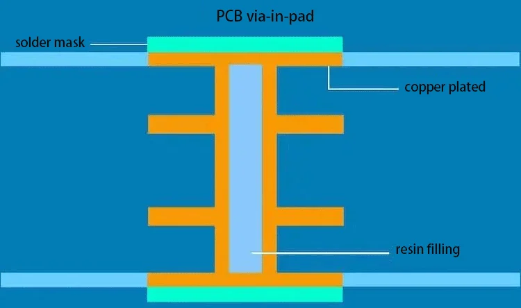
A PCB via-in-pad includes a PCB hole and a pad. The hole is plated with copper for conductivity between the desired layers and then filled with resin to prevent the solder from flowing into the hole. The pad is applied with a surface finish such as immersion gold or OSP for soldering.
Situation to Use Via-in-Pad in Your PCB
In principle, it's not recommended to drill the PCB hole on the pad, as it may lead to the non-soldering issue during reflow soldering.
However, for a BGA with a large number of pins, via-in-pad is the cure for PCB wiring, saving space and improving signal integrity. Besides, PCB via-in-pads increase thermal dissipation.
When do you consider via-in-pads in your PCB? Below are the situations to use via-in-pads.
1. Wiring for BGA and HDI PCB
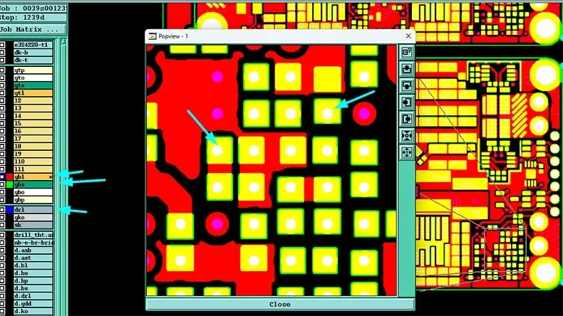
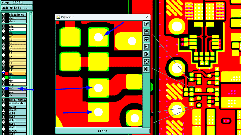
A ball grid array has multiple solder balls, so its PCB footprint should have an array of PCB pads for the corresponding solder balls. If the BGA pitch is 0.8mm and above, the traditional wiring way - dog bone fanout, which uses short traces to connect the BGA pad to the via outside the footprint and lead the signal to the inner layer, can work.
However, if the BGA pitch is below 0.65mm, especially 0.5mm and below, for PCB wiring, via-in-pads are needed. For HDI PCBs with an SMD pitch of 0.65mm and below, via-in-pads are also needed.
These vias in the pads in the BGA PCB footprint and HDI PCBs are blind vias. They connect the BGA or other fine-pitch SMD on the pad to the desired PCB inner layer. They reduce the routing complexity and increase thermal dissipation.
2. Wiring for high-speed signals
For PCB wiring for high-speed and high-frequency circuits, such as USB, HDMI, and a DDR4 memory module, via-in-pads enable the signal lines to be shorter.
A high-speed circuit requires strict impedance control and signal symmetry. For a high-speed circuit, regular through holes may bring parasitic inductance and capacitance, causing signal reflection.
By using via-in-pads, it gets shorter for the signal to pass the via, reducing signal distortion.
However, if you don't use a via-in-pad, it's also okay, as you can remove the stub of the through hole with back drilling in the PCB fabrication process to reduce signal reflection.
3. Thermal management for high-power components
Another reason to use via-in-pads in a PCB is thermal management, as the SMD component is directly connected to the heat dissipation layer.
For high-power BGAs such as CPU, GPU, and FPGA, MOEFET, or DC-DC converter, thermal management is a must. If you apply via-in-pads, heat generated by these high-power components can dissipate to the large copper layer in the PCB, such as a PCB busbar. It efficiently conducts heat from the high-power SMD.
How to Make PCB Via-in-Pads
Via-in-pads in a PCB can be a through hole or blind hole. The drilling and plating process for making via-in-pads is below.
Step 1. Drilling the through hole or blind hole
First, a through hole is drilled by mechanical drilling, or a blind hole is drilled by laser in the PCB. Right now, the pad is not made yet, so there are no worries about whether drilling can affect the pad.
Step 2. Copper plated the hole
The through hole or blind via is plated with copper to connect the desired PCB layers.
Step 3. Resin filling the via
The through hole or blind via is filled with epoxy resin to prevent the solder from going into the hole. When the liquid resin fills the hole, it is baked to cure.
Step 4. Flattening the resin
When the resin in the hole is cured, remove the excessive resin and grind to flatten the surface of the resin.
Step 5. Hole copper capped and making the pad
Here comes the second time for copper plating the hole. The hole surface is plated to be capped with copper.
Besides, the pad is created by copper plating.
Step 6. Applying a surface finish onto the pad
Finally, the via-in-pad is applied with a surface finish. ENIG and OSP are the common surface finishes for via-in-pads.
Turnkey Advanced and HDI PCB Manufacturer with Via-in-Pads Capabilities
If your PCB or PCBA project needs via-in-pads, no matter it is through hole or blind via in the pad, you can work with the advanced PCBA manufacturer PCBONLINE from R&D to one-stop PCBA manufacturing.

Founded in 1999, PCBONLINE has R&D capabilities for HDI projects and EMS manufacturing capabilities. It provides 4-to-64-layer HDI PCB fabrication, assembly, and PCBA box-build assembly. You can order various multilayer PCBs requiring via-in-pads from PCBONLINE, such as FR4 PCBs, HDI PCBs, rigid-flex PCBs, and high-frequency PCBs.
PCBONLINE can deal with via-in-pads, via filling, via tenting, and back drilling.
All types of PCB vias can be handled by PCBONLINE, such as through holes, via-in-pads, microvias, staggered/stacked blind vias, buried vias, etc.
PCBONLINE provides free and professional DFM (design for manufacturing) for PCB, PCBA, and box-build projects before and during prototyping/sampling to ensure the success of your project and seamless mass production.
Besides multilayer PCB fabrication, we have powerful capabilities in fine-pitch assembly for HDI PCB assembly.
High-quality multilayer and HDI PCBA manufacturing certified with ISO 9001:2015, ISO 14001:2015, IATF 16949:2016, RoHS, REACH, UL, and IPC-A-610 Class 2/3.
PCBONLINE will ensure the success of your project that requires via-in-pads, solve all issues, and provide smooth BGA reballing and PCBA manufacturing.
Here are the PCB via-in-pad capabilities at PCBONLINE:
- Finished hole size for via-in-pad filling with resin: 0.1-0.9mm (drill size 0.15-1.0mm), 0.3-0.55mm normal (drill size 0.4-0.65mm)
- Max aspect ratio for via-in-pad filling with resin PCB - 12: 1
- Min resin plugged PCB thickness: 0.2mm
- Max via-filling ith resin PCB thickness: 3.2mm
- Making different hole sizes with via filling in one board: Yes
No matter what application your project will be used for, such as automotive, industrial control, medical, military, aerospace, communication, computer, etc, you can work with PCBONLINE. To reach out to the OEM PCB manufacturer PCBONLINE, contact info@pcbonline.com.
Conclusion
This blog introduces what a PCB via-in-pad is comprehensively. Multilayer PCBs and HDI PCBs, especially those with the BGAs, may use via-in-pads. To ensure the success of your PCB/PCBA projects requiring via-in-pads, work with the turnkey advanced PCB manufacturer PCBONLINE.
PCB fabrication at PCBONLINE.pdf


