
Radio Frequency (RF) circuit boards are at the core of wireless communication devices, from smart homes to industrial IoT. Designing RF PCBs goes beyond FR4 circuit boards—it involves specialized materials, precise impedance control, and careful attention to manufacturing quality.
In this blog, we'll explore the key elements of RF PCBs, highlight common mistakes to avoid, and walk through a practical example—designing an antenna for ESP32.
What Makes RF PCBs Different?
RF PCBs operate at high frequencies, typically in the MHz to GHz range, where signal behavior is sensitive to design imperfections. Standard PCB materials and layout practices often fail at these frequencies, leading to signal loss, reflection, and interference.
That's why RF PCBs require low-loss materials, impedance-matched traces, and high manufacturing precision to maintain performance.
1. Selecting the Right Material
The choice of PCB material significantly impacts signal quality in RF designs. Materials must support low signal loss, stable dielectric properties, and thermal consistency. Using standard FR4 beyond certain frequencies can result in degraded performance, so RF-specific laminates are often necessary.
Here are some critical properties and options to consider:
Key material properties:
- Dielectric constant (Dk): Affects signal speed and impedance. Should be low and stable.
- Dissipation factor (Df): Indicates signal loss. Lower Df means better performance.
- Thermal stability: Ensures consistent performance across temperatures.
Common RF materials:
- Rogers 4350B/4003C: High-performance, commonly used for frequencies up to 10 GHz.
- Taconic RF-35: Cost-effective, good for mid-range RF applications.
- PTFE (Teflon-based materials): Excellent performance but challenging to manufacture.
- FR4: Acceptable for low-frequency RF (e.g., 2.4 GHz Wi-Fi) with some trade-offs.
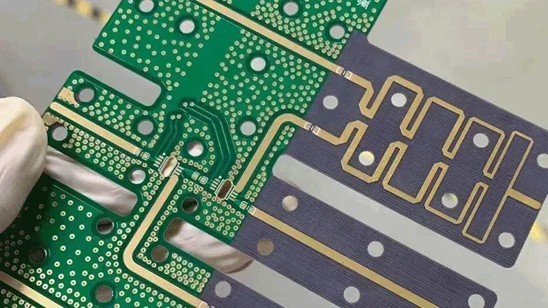
Impedance Control: Key to Signal Integrity
In RF design, maintaining consistent impedance along signal traces is crucial. Mismatched impedance leads to signal reflections, loss, and poor wireless performance.
Designers must calculate trace widths and spacing carefully, considering the PCB's material and stack-up.
Impedance control tips:
- Use transmission line structures like microstrip or coplanar waveguide.
- Calculate trace widths for 50Ω impedance (common standard for RF circuits).
- Account for copper thickness and dielectric height in your calculations.
- Ensure tight manufacturing tolerances, especially ±0.02mm trace width accuracy.
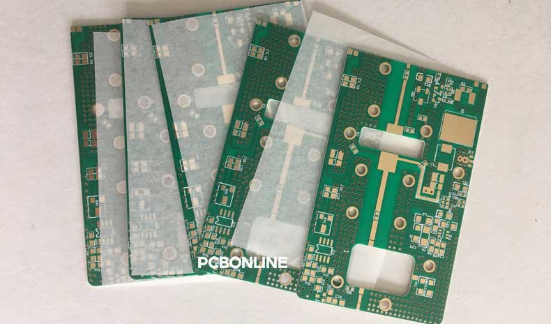
Key Manufacturing Considerations
RF PCBs require precision manufacturing to maintain signal integrity and long-term reliability. Standard fabrication processes may not suffice, so it's essential to choose a high-frequency PCB manufacturer PCBONLINE that understands RF requirements.
Below are some key manufacturing techniques that enhance RF PCB quality:
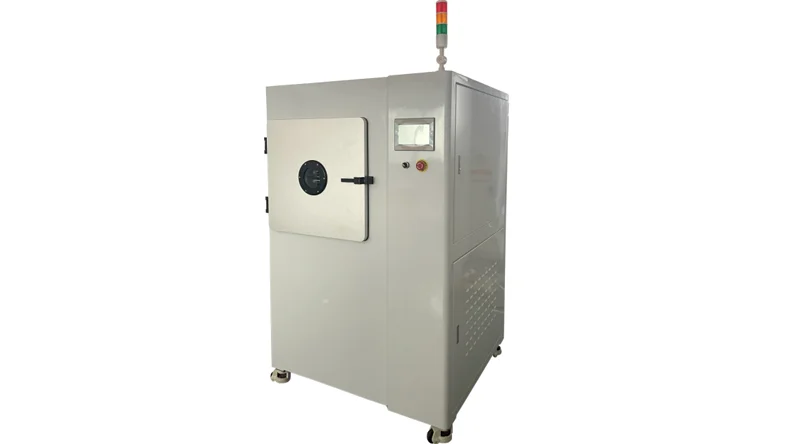
- Plasma cleaning: Removes all residues and ensures clean plated holes—critical for RF performance.
- Thermal shock testing: Confirms that hole walls don't separate under temperature changes.
- Copper compensation: Ensures trace widths remain within ±0.02mm tolerance, maintaining impedance consistency.
Common Mistakes in RF PCB Design (Avoid These!)
Even well-designed RF circuits can fail due to avoidable errors in layout or material choice. Below are common pitfalls to avoid.
1. Ignoring controlled impedance
Designers sometimes use default trace widths without considering their effect on impedance. This leads to signal reflections.
Solution: Always calculate and verify trace widths for 50Ω impedance using calculators or stack-up data.
2. Poor grounding
Inadequate or fragmented ground planes result in noise, EMI issues, and degraded RF performance.
Solution: To minimize interference, use a continuous, solid ground plane beneath RF traces and components.
3. Long RF traces
Long traces introduce signal loss and timing issues, especially at GHz frequencies.
Solution: Minimize trace length and keep RF signals as short and direct as possible.
4. Excessive use of vias
Every via on an RF trace disrupts impedance, causing signal degradation.
Solution: Avoid vias in RF paths unless necessary. If used, maintain impedance continuity through via design.
5. Component placement near the antenna
Placing components or copper pours too close to the antenna detunes it, reducing performance.
Solution: Leave a clear zone around the antenna for proper radiation. Follow antenna design guidelines for spacing.
6. Ignoring fabrication tolerances
Failing to account for trace width and spacing tolerances leads to inconsistent impedance.
Solution: Work with manufacturers who guarantee tight tolerances—especially ±0.02mm trace width control.
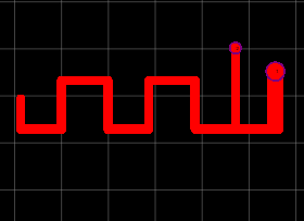
RF PCB Example: a PCB Antenna for ESP32
Let's now walk through a real-world example—designing a 2.4 GHz PCB antenna for the popular ESP32 Wi-Fi/Bluetooth module.
Instead of designing a complete board, we'll focus only on routing the antenna.
Step 1: Choose antenna type
For 2.4 GHz, common antennas include:
- Inverted-F antenna (IFA): Compact, reliable, and widely used with ESP32.
- Meandered line antenna: Fits in tight spaces, decent performance.
- Straight Monopole antenna: Easy to design but larger.
We'll design an Inverted-F Antenna (IFA) for a good balance of size and efficiency.
Step 2: Design in a PCB layout tool
1. Open any PCB layout tool and start a new PCB layout.
2. Draw the antenna trace on the edge of the PCB for optimal radiation.
3. Connect the feed point to the ESP32's RF pin (commonly labeled ANT).
4. Add an optional matching network (capacitor/inductor) for fine-tuning.
5. Ensure no ground plane under the antenna, and maintain clearance from components.
Step 3: Calculate trace width for 50Ω impedance
For FR4 material (1.6mm thickness, 35µm copper), a microstrip trace width for 50Ω impedance is approximately 2.9mm. Use an impedance calculator for precise width based on your stack-up.
Step 4: Final checks
- Run DRC (Design Rule Check) in the PCB layout tool.
- Export Gerber files.
- Specify to your manufacturer that the antenna trace must meet 50Ω impedance and follow tight tolerance requirements.
Antenna Design Example
Here's a snapshot of the routed Inverted-F antenna for ESP32:
One-stop RF PCB Manufacturer with R&D Capabilities
Whether you're working on an IoT device, wireless sensor, or custom ESP32 module, the RF PCB manufacturer PCBONLINE will help you build reliable wireless devices under one roof.
PCBONLINE is a high-speed and high-frequency PCB manufacturer and assembler founded in 1999. It has two large advanced PCB manufacturing bases, one PCB assembly factory, stable supply chains, and an R&D team.

Provide one-stop radio-frequency PCB manufacturing, including R&D, prototyping, PCB fabrication, component sourcing, PCB assembly, PCBA value-added, and box-build assembly.
Equipped with complete machines for Plasma cleaning and thermal shock testing.
PCBONLINE grasps the core technologies for RF PCB manufacturing, such as copper compensation, impedance control, embedded antenna DFM, expansion/contraction control, etc.
Have ready-to-use RF PCB base materials in stock, and the storage period is within 45 days to ensure the best performance of the RF circuit boards (at manufacturers who have no storage, it usually takes 2 to 3 months to purchase these base materials).
High-quality radio-frequency PCB manufacturing certified with ISO 9001:2015, ISO 14001:2015, IATF 16949:2016, RoHS, REACH, UL, and IPC-A-600 Class 2/3.
PCBONLINE pays attention to quality and cost-effectiveness in RF PCBs. If you want to get a quote or ask questions, you can send emails to info@pcbonline.com to get a quote.
Conclusion
RF circuit boards require more precision and EMI shielding than standard PCBs. Material selection, impedance control, and precise manufacturing are essential to ensure signal integrity and wireless performance of RF PCBs. By avoiding common mistakes and using a PCB design tool, you can design effective antennas and RF circuits for your projects. If you need radio-frequency PCBs or PCBA, work with the one-stop PCBA manufacturer PCBONLINE.
PCB fabrication at PCBONLINE.pdf


