
In the field of electronic manufacturing, many people often confuse the concepts of SMD and SMT. This blog will help you understand what SMD and SMT are and how to choose in electronic manufacturing.
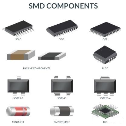
SMD stands for Surface Mount Device. Common ones include resistors, capacitors, BGA, etc. They are small and suitable for circuit boards that require high-density assembly.
So, what is the relationship between SMD and PCB assembly technology? This article will reveal the specific process of SMD PCB assembly.
What is SMD?
Surface mount devices (SMDs) are components used in the SMT (Surface Mount Technology) assembly process to adapt to PCBs that require small design and high density. Different from traditional through-hole technology (THT), SMD components do not need to be installed through holes in the PCB but are fixed to the PCB surface through solder paste and reflow soldering process.
Specific steps of SMD PCB assembly
1. Component Inspection
The manufacturer's SMDs are purchased. That's why they need to be inspected. First, all SMD electronic components need to be inspected, including all PCBs and their specifications. The engineering department checks that the package, shape and volume of the SMD PCB components should be consistent with the provided BOM file, and whether the PCB to be installed is good. Only when everything is confirmed to be fine can it be prepared for processing.
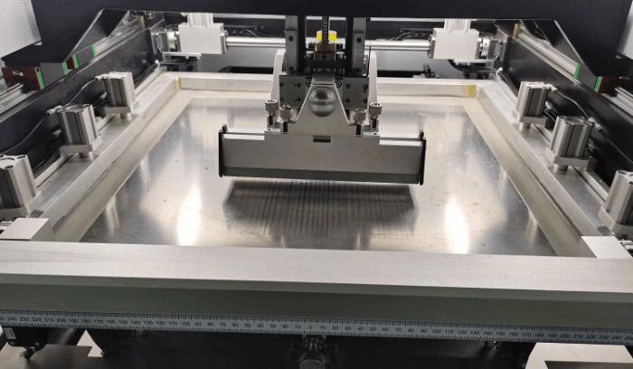
2. Solder Paste Printing on the PCB
The PCB and laser-cut steel mesh are precisely aligned and fixed, and the solder paste is pushed to fill the steel mesh openings with a scraper at a specific pressure and speed. The steel mesh is then quickly demolded and separated so that the solder paste is evenly deposited on the PCB pads. Finally, optical inspection (SPI) is used to verify the thickness and shape of the solder paste to ensure that there are no defects such as offset and bridging.
3.Pick and Place
Through precise steel mesh placement, solder paste is printed on circuit boards, and after inspection, the quality is good. After that, the high-precision placement machine firmly attaches the prepared SMD components to the printed circuit board printed with solder paste. The Pick-and-Place Machine uses a vacuum nozzle to place SMD components onto solder paste at high speed and high precision.
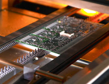
4.Reflow Soldering
The key to reflow soldering is to match the temperature curve of solder paste characteristics (such as melting point) and component temperature resistance, which is usually divided into 4 stages:
(1) Preheat Zone
Temperature range: room temperature → about 150°C
Heating rate: 1~3°C/s (too fast will cause solder paste to splash and form solder beads).
Purpose:
Evaporate the solvent (flux) in the solder paste.
Slowly increase the temperature to avoid thermal shock that may cause PCB or component cracking.
(2) Soak Zone
Temperature range: 150~180°C
Time: 60~120 seconds
Purpose:
Make the overall temperature of the PCB and components uniform and reduce temperature differences.
Activate the flux and remove oxides on the surface of the pads and component pins.
(3) Reflow Zone
Temperature range: above the melting point of solder paste (lead-free solder paste: 217~250°C).
Peak temperature: usually 20~30°C higher than the melting point of solder paste (e.g. Sn-Ag-Cu lead-free solder paste has a melting point of 217°C and a peak temperature of about 240~250°C).
Time: Maintain peak temperature for 40 to 90 seconds (too long will cause thermal damage to components).
Purpose:
The solder paste is completely melted to form an intermetallic compound (IMC) for reliable soldering.
The surface tension of the molten solder paste causes the components to automatically align with the pads (Self-Alignment Effect).
(4) Cooling Zone
Cooling rate: <5°C/s (too fast cooling will cause solder joint brittleness or residual stress).
Purpose:
Control the solidification process of the solder joint to form a dense structure.
Avoid internal damage to the component due to sudden cooling (such as micro cracks in ceramic capacitors).
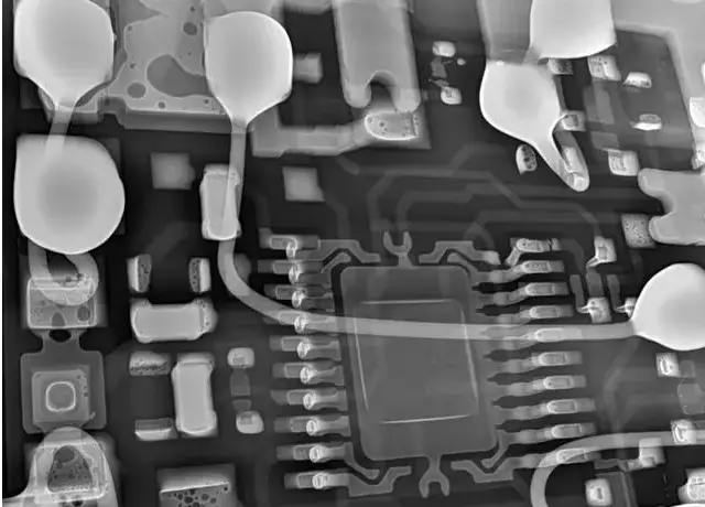
5. Inspection & Testing
After the circuit boards are completed, they will enter a series of inspection procedures:
AOI (Automatic Optical Inspection)
Inspect the quality of solder joints (virtual soldering, offset, bridging, etc.) through multi-angle cameras.
X-ray Testing
Used for internal structure analysis of hidden solder joints such as BGA and QFN.
FCT (Functional Circuit Test)
Simulate actual working conditions and verify circuit performance (such as voltage and signal integrity).
ICT (In-Circuit Test)
Test the electrical parameters of key nodes through probes.
The above is the specific process of SMD in PCB assembly, and the actual assembly process will be adjusted according to the orders of different industry segments.
One-Stop HDI PCB Manufacturer and Its PCB Via Filing Capabilities
If you're looking for turnkey HDI electronics manufacturing services (EMS) from hardware development to PCBA fabrication and box-build assembly, you can work with the one-stop HDI PCBA manufacturer PCBONLINE.
Founded in 1999, PCBONLINE has R&D capabilities for HDI projects and EMS manufacturing capabilities, including via filling for stacked vias. It provides 4-to-64-layer HDI PCB fabrication, assembly, and PCBA box-build assembly. You can order various HDI PCBs from PCBONLINE, such as FR4, polyimide (flexible PCB), polyimide + FR4 (rigid-flex PCB), and PTFE/Rogers (high-frequency PCB).

3000m² of production capacity per day for HDI PCBs with builds of 1+N+1, 2+N+2, 3+N+3,4+N+4, and arbitrary interconnection in any layers.
PCBONLINE has hardware and software R&D capabilities for IoT applications requiring HDI design, including PCBA and enclosures.
We can manufacture complex PCBs with stacker vias, via-in-pad, microvias, inlay boards, heavy copper designs, and hybrid and fine structure lay-ups.
Besides HDI PCB fabrication, we have powerful capabilities in fine-pitch assembly for HDI PCB assembly.
We have rich R&D and manufacturing experience for HDI applications such as FPGA boards.
High-quality HDI PCB and PCBA manufacturing certified with ISO 9001:2015, IATF 16949, RoHS, REACH, UL, and IPC-A-610 Class 2/3.
Here'e the PCB via filing capabilities at PCBONLINEL:
- Micriavia filling with copper: laser via size 0.1-0.125mm, priority 0.1mm
- Finished hole size for via-in-pad filling with resin: 0.1-0.9mm (drill size 0.15-1.0mm), 0.3-0.55mm normal (drill size 0.4-0.65mm)
- Max aspect ratio for via-in-pad filling with resin PCB - 12: 1
- Min resin plugged PCB thickness: 0.2mm
- Max via-filling ith resin PCB thickness: 3.2mm
- Making different hole sizes with via filling in one board: Yes
- Via filling with copper/silver: Yes
If you need HDI PCBAs or any other PCBAs requiring via filling, please send your email to PCBONLINE at info@pcbonline.com. We will provide one-on-one engineering support to you.
Conclusion
Via filling is used for creating stacked vias in HDI PCB fabrication, BGA/CSP/QFN IC packaging, and filling PCB via-in-pad with resin during multilayer PCB fabrication. If you need one-stop electronics manufacturing for your HDI PCBA project, contact the one-stop advanced PCB manufacturer PCBONLINE for high-quality PCBA and box-build solutions tailored to your project's needs.
PCB fabrication at PCBONLINE.pdf


