
Wave soldering is a soldering technology to solder through-hole components firmly to the PCB PTH hole walls. In this blog, we will get an insight into wave soldering, five problems that may occur during wave soldering, and our solutions to solve them one by one.
In this article:
Part 1. What is Wave Soldering? Part 2. PCB Wave Soldering Issues and Solutions to Them Part 3. One-stop PCB Assembly Manufacturer PCBONLINEWhat is Wave Soldering?
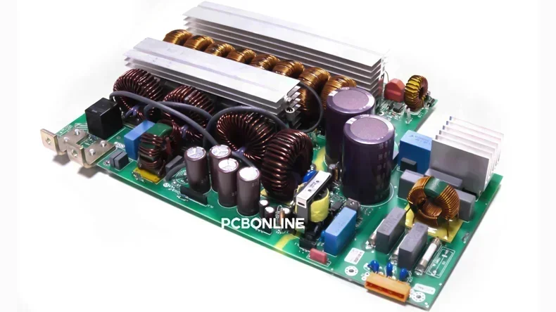
Wave soldering is passing the underside of the PCB through the molten solder wave to connect the PTH components to the printed circuit board. Almost all PCB boards using PTH components require wave soldering in PCB assembly.
One-wave soldering:
One-wave soldering is used rarely nowadays. It is used for simple PCB boards. The soldering side of the PCB passes over a single wave of molten solder.
Two-wave soldering:
The front wave crest is a fast-moving solder wave, which washes away the flux that is trapped behind the PTH components due to the "shielding effect". So the solder joints can be reliably lubricated. The second solder wave is a rear wave crest, which further trims the lubricated but irregularly shaped solder joints to make them perfect.
Wave Soldering Process Step by Step
What is the wave soldering process? Please check the process below.
Step 1. Preparation
Place the PCBA in the jig, which wraps the PCBA and only exposes the PTH hole areas for soldering.
The jig is custom-designed by the PCBA manufacturer and made by the mold factory it cooperates with according to the PCBA manufacturer's design and requirements.
Working with an experienced PCBA manufacturer PCBONLINE that can design the jig properly can get rid of many wave soldering issues. This will be revealed in the next parts.
Then place the PCBA with the jig onto the conveyor rails of the wave soldering machine to start wave soldering.
Step 2. Flux application
The wave soldering process is automatic from this step. All the process time and speeds are controlled by the machines according to the specs set up by the PCBA manufacturer.
Apply flux to the bottom side of the PCB, where the through-hole leads are located.
Step 3. Preheating
The PCB goes to the preheating zone. Here the PCB's temperature gradually goes up until it can meet the molten solder without thermal shock.
Preheating also activates the flux, which can alleviate soldering.
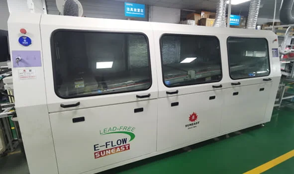
Step 4. Solder wave contact
The PCB goes into the wave soldering oven. In the oven, a bucket of molten tin is stirred to get a continuous wave.
As the PCB moves over the molten solder wave, and the PTH component leads that protrude the holes are exposed to the molten solder.
The solder flows into the holes and around the component leads, filling the space between the lead and the hole walls.
Step 5. Cooling, trimming, and cleaning
After soldering, the PCB leaves the wave soldering machine and cools down naturally.
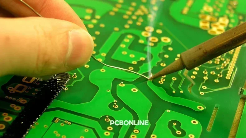
A technician will trim the PTH component leads to be 1mm to 2mm, and the next technician will check the board visually and remove the flux residue from the PCBA.
The above is all the wave soldering process. As wave soldering is a bulk soldering process that solders all the PTH components at one time, some issues may occur. Check them one by one and our solutions to prevent them!
PCB Wave Soldering Issues and Solutions to Them
Below are the common issues that may occur during the wave soldering process and their solutions.
PTH component floatation
During wave soldering, the PTH component may go up to the top side like floating (as shown in the diagram), leading to gaps and uneven surfaces between the component lead and the PCB hole walls.
The PTH component floatation issue arises from improper manual component placement and the thermal expansion of solder paste during soldering.
PCBONLINE's solutions are straightforward:
First, when designing the jig/fixture, we ensure they not only protect components from high temperatures but also press down on components prone to movement.
Second, for components requiring high positional accuracy, such as buttons or sockets that must align precisely with the enclosure, we apply a layer of adhesive to the component's bottom before soldering.
Alternatively, we can select selective soldering to prevent soldering defects and component displacement.
Solder spikes or protrusions

Solder spikes or protrusions refer to the sharp or pointed solder formations on the trimmed PTH component lead or tin-intake path. It can affect the safety space and pierce the PCB solder mask.
The causes of these issues during wave soldering can be:
- A metal PTH component in a relatively large size s absorb heat, leading to uneven heat absorption.
- Too long PTH component lead
- Insufficient preheating
- Insufficient tin temperature
- The PCB passing the furnace too fast
- Uneven temperature conduction of hand-soldering iron
How do we fix the solder spike issue?
First, increase the preheating temperature, reduce the PCB passing oven speed, and increase the molten tin temperature.
Second, trim the lead length within 2.5mm.
Third, increase the solder ion temperature or replace the soldering iron tip with a larger heat conduction area.
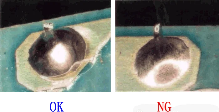
Pinholes

The pinhole issue refers to the pinhole-sized holes on the surface of the solder joint. It leads to poor appearance and poor solder joint strength.
The causes of pinholes include:
- The PCB contains moisture.
- The component lead is contaminated (such as by silicone oil).
- The air in the through hole is blocked by the component and doesn't escape.
How to fix the pinhole issues?
First, bake the PCB at 80℃-100℃ for 2-3 hours before wave soldering if it has been stored for quite a long time.
Second, don't touch the PCB surface at any time to avoid contamination.
Third, change the molding method of the PTH component to prevent the coating from falling into the hole, or check the matching of the hole diameter and wire diameter to see if there are air holes.
Insufficient soldering
The solder may not cover the entire PTH hole pad, and the soldering height is lower than required. It can lead to not enough soldering strength and tin cracks when subjected to external force and affect the PCBA service life.
The causes of insufficient soldering are:
- Too high tin temperature, too large angle when passing through the oven, too high or too low flux density, and too low backplate
- Too long PTH component leads
- Unmatched solder pad (too large) to the wire diameter
- Too close solder pads, resulting in tin pulling
The solutions include:
First, adjust the solder pot.
Second, shorten the wire pins.
Third, change the pad design in the PCB layout.
Fourth, add solder mask to separate the pads.
Excessive soldering

Excessive soldering means too much tin in the solder joint making the solder joint protrude outward. It does not help with the current conduction but weakens the strength of the solder joint.
The reasons can be:
- Too low soldering temperature, too short soldering time.
- Insufficient preheating temperature, resulting in not full activation and cleaning effect of the flux.
- Too low ratio of the flux.
- Too small angle when the PCB passes the wave soldering oven.
How do we solve this issue?
First, increase the tin temperature or slow down the furnace speed.
Second, adjust the preheating temperature.
Third, adjust the Flux ratio.
Fourth, adjust the PCB passing tin oven angle.
One-stop PCB Assembly Manufacturer PCBONLINE
PCBONLINE is a high-quality PCBA manufacturer providing SMT and PTH assembly. We focus on advanced PCB fabrication, PCB assembly, PCBA value-added, and box-build assembly from prototypes to mass production.

Founded in 1999, PCBONLINE has two large advanced PCB manufacturing bases, one PCB assembly factory, an R&D team, and stable supply chains. Besides, it has strategic cooperation with the top 3 mold factories in China to fabricate the jigs, molds, and SMT stencils for PCB fabrication, SMT assembly, and wave soldering.
PCBONLINE will design the jig properly for wave soldering avoiding the floatation issue.
Besides wave soldering, PCBONLINE provides selective soldering as an advanced alternative for PCBs with thermal sensitivity components.
PCBONLINE has rich experience in wave soldering oven temperature and speed control to prevent the above-mentioned soldering issues.
High-quality PCBA manufacturing certified with ISO 9001:2015, ISO 14001:2015, IATF 16949, RoHS, REACH, UL, and IPC-A-610 Class 2/3.
When your project goes to the bulky production stage, we will return the fees of prototyping/sampling and R&D and offer free PCBA functional testing and program burn-in.
We offer one-on-one engineering support for each project throughout the process. To communicate with the OEM PCB manufacturer PCBONLINE, contact info@pcbonline.com.
Conclusion
Wave soldering provides electrical connectivity and physical durability between the PTH components and the PCB. This article introduces the wave soldering step-by-step process and common issues that may happen during wave soldering. PCBONLINE is a one-stop PCBA manufactured with rich experience in wave soldering. Email contact or chat online with PCBONLINE for your project and get one-on-one professional engineering support now.
PCB assembly at PCBONLINE.pdf


