
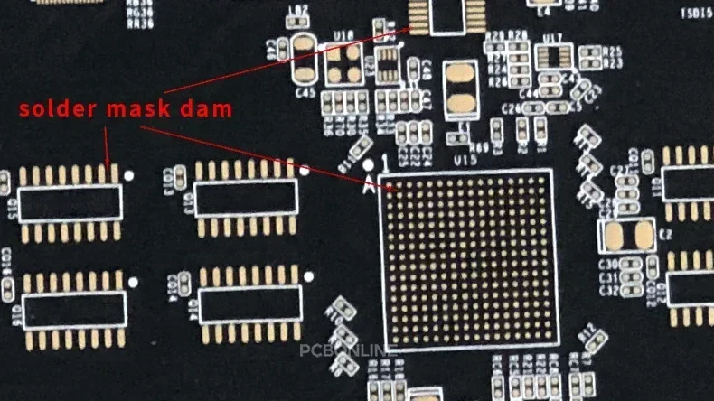
black solder mask between the exposed copper pads represents the solder mask dam
What does "Dam" mean in a PCB (printed circuit board)? Usually, the PCB dam refers to the solder mask dam. However, for a waterproof PCB, it may also refer to the dam and fill encapsulation. This article explores the solder mask dam and dam-and-fill PCB to learn about all these terms.
In this article:
Part 1. What is Solder Mask Dam? Part 2. What is PCB Dam and Fill? Part 3. Function of Solder Mask Dams Part 4. Key Terms Related to Solder Mask Dams Part 5. When and How to Use a Solder Mask Dam? PCB Dam Hassle-free with the Advanced PCB Manufacturer PCBONLINEWhat is Solder Mask Dam?
SMT and PTH soldering is the process of connecting electronic components to the exposed copper areas of the PCB, by melting a filler metal called solder. When molten solder is placed on the PCB during the soldering process, it sometimes flows into surrounding areas, especially in closely spaced pins or pads. To solve this problem, the solder mask dams come into play. It stops the solder from making unwanted connections between pads or traces.
Solder mask dam or solder mask bridge refers to a thin barrier formed by a solder mask that separates areas of exposed copper. The dam is created to prevent solder from flowing across areas where it isn't wanted during the assembly process. Usually, the dams are of around 4 mil (0.1 mm) or more, but mostly depend on manufacturing capabilities.
What is PCB Dam and Fill?
Another meaning of PCB dam is PCB dam and fill encapsulation. It is a waterproofing method using a quick-drying resin to build a small containment barrier (a dam) around the targeted components on the PCB. Once cured, the melting silicon or epoxy resin is poured into the dam and then baked to cure.
PCB dam-and-fill encapsulation is way different from the solder mask dam, so when you come across the term PCB dam, make sure you understand what it is in the context.
In most cases, a PCB dam refers to a solder mask dam. Learn more about a solder mask dam in the below content.
Function of Solder Mask Dams
To understand why solder mask dams make a difference in the life of PCBs, let us discuss their key functions. A solder mask dam produces a separation between tightly spaced pads or traces as the solder mask itself is not conducive and thus prevents any undesired connections from forming during the soldering process. These solder mask dams are useful for:
- Migrating the risk of producing solder bridges and electrical shorts during the soldering process. A solder bridge is an unintended electrical connection that is formed while soldering the PCB and causes electrical shorts which can cause the circuit to behave abnormally.
- Enhancing the accuracy of the soldering process by preventing unintended connections. The correctly soldered PCB will work properly according to the design while a board that went through an inaccurate soldering process will not.
- Offering enhanced design flexibility within PCB design using the assistance of various layouts of components and the soldering processes. The solder mask dams ensure the accuracy of the soldering process even with highly complex components.
- A cleaner soldering process prevents the possibility of solder bridging between adjacent conductive features which ultimately prevents the PCBs from malfunctioning.
Key Terms Related to Solder Mask Dam
Now that we have understood the concept of solder mask dams, there are some technical terms that you need to know for further understanding of when and how to use solder mask dams.
Pitch:
It is the center-to-center spacing between two adjacent holes or pads on the Printed Circuit Board.
Till now, we have used terms like "closely spaced pads" or "tightly spaced pads" which means the pins or pads of the components are very near to each other. In technical terms, this is called "fine pitch" which means there is a very small spacing between the pads of the components.
Typically, surface mount devices (SMDs) with a pad-to-pad spacing of 0.65mm or less are considered fine-pitched.
Solder mask opening:
The solder mask opening refers to the exposed copper area for soldering and is not covered by the solder mask.
It is designed to position and properly size the solder mask opening to allow a seamless soldering process and prevent unwanted bridging. The solder mask opening is not covered by the solder mask to still be able to solder. This makes sure that the pads are properly exposed for soldering.
Solder mask clearance:
While it is important to understand what solder mask dams are, it is equally essential to distinguish them from solder mask clearance.
We now know that the solder mask dam is a localized area of the solder mask material on the PCB between fine-pitched pads and is used to prevent solder bridging between adjacent pads during the soldering process.
The solder mask clearance, on the other hand, refers to the spacing between the pad edge and the solder mask opening.
A solder mask's clearance must be precise because a small size can lead to mask overlap and a larger size could result in solder bridging. Typical solder mask clearance is often 2–4 mils (0.05–0.1 mm) larger than the pad to ensure full exposure to the solder. The following image shows the solder mask clearance in the PCB's edge connectors for clarity.

When and How to Use a Solder Mask Dam?
Normally, the solder mask dams are applied to the electronics components having a pitch of 0.2mm or greater. This spacing allows the designers to carefully place the solder mask dams between the pads to provide insulation. With components having a pitch of less than 0.2mm, there isn't much space left for placing the dams. Therefore, the entire footprint is left for soldering to accommodate all pads.
Electrostatic spraying is the process where an electric field is used to apply the solder mask on the PCB surface.
Similarly, the liquid photimageable (LPI) is the technique in which a UV-sensitive liquid solder mask is applied across the board, which is then exposed to ultraviolet light through a photomask, masking the overall board except for the precisely exposed areas.
Both techniques are high-precision application methods of solder masks and are utilized where traditional silkscreen printing lacks.
PCB Dam Hassle-free with the Advanced PCB Manufacturer PCBONLINE
If you're looking for a professional PCB manufacturer that can deal with PCB dams and any other details for your project, you can work with the advanced PCB manufacturer PCBONLINE from R&D to one-stop PCBA manufacturing and box-build assembly from prototypes to bulky production.

Founded in 1999, PCBONLINE has two large advanced PCB manufacturing bases, one turnkey PCB assembly factory for PCB assembly and box-build assembly, stable material supply chains and strategic cooperation with electronic component manufacturers, and long-term cooperation with the top 3 mold and enclosure manufacturers in China for jigs/fixtures, molds, and enclosures.
Besides, PCBONLINE has an R&D team and professional CAM engineers for project development and DFM (design for manufacturing).
PCBONLINE can apply solder mask dams, dam and fill encapsulation, solder mask openings, solder mask clearance, etc, to PCBs according to your project.
No matter what your PCB requirements are, such as fine-pitch BGA, waterproof, edge connectors, etc, PCBONLINE can meet your PCB demands.
PCBONLINE manufactures, assembles, and tests from PCBs to box-builds as a source factory manufacturer under one roof, from prototypes to bulky production.
Complete PCBA value-added services in the post-assembly stage, including PCB coatings, functional testing, thermal aging, IC programming, box-build assembly, and application simulation testing.
Provides one-on-one free and professional DFM (design for manufacturing) for PCB, PCBA, and box-build projects before and during prototyping/sampling to ensure the success of your project and seamless mass production.
High-quality PCBA manufacturing certified with ISO 9001:2015, ISO 14001:2015, IATF 16949:2016, RoHS, REACH, UL, and IPC-A-610 Class 2/3.
When your project enters the bulky production stage, PCBONLINE refunds the fees of prototyping including its value-added services.
By working with the one-stop PCBA manufacturer PCBONLINE, you don't need to find other providers for value-added services, as all procedures, components, tests, jigs, and enclosures can be provided by PCBONLINE. No matter what application your PCB will be used for, such as automotive, industrial control, medical, military, aerospace, communication, agriculture, etc, you can work with PCBONLINE. To reach out to the turnkey PCBA manufacturer PCBONLINE, contact info@pcbonline.com.
Conclusion
The solder mask dams are used to prevent solder from bridging between fine pitch pads or traces during the SMT soldering process. They ensure a clean and reliable soldering process by stopping the solder bridges from forming. The formation of solder mask dams during the PCB manufacturing process requires accuracy, alignment, and durability which is often achieved by electrostatic spraying and liquid photimageable solder masks. To ensure the success of your PCB/PCBA projects requiring PCB dams, work with the turnkey advanced PCB manufacturer PCBONLINE.
PCB fabrication at PCBONLINE.pdf


