![]()
HDI stands for high-density interconnect, which means the circuit board has an extremely high density of circuit connection. To achieve HDI, the PCB has to have extremely small PCB vias and fine traces. We call these circuit boards HDI PCBs. In this article, you will learn what an HDI PCB is, its structures, and its manufacturing.
Part 1. What is an HDI PCB
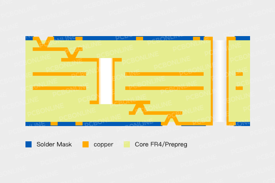
An HDI PCB is a multilayer circuit board with microvia diameter within 5mil (0.127mm), line space/width of inner and outer circuit layers within 4mil (0.10mm), and PCB pad diameter within 0.35mm. For HDI PCBs, microvias can be single microvias, staggered vias, stacked vias, and skip vias, and because of microvias, HDI PCBs are also known as microvia PCBs. HDI PCB features blind microvias, fine traces, and sequential lamination manufacturing.
If you don't know the mentioned PCB vias for HDI PCBs, please refer to this post: 8 Types of PCB vias - A Complete Guide of PCB Vias in 2021.
HDI PCBs are usually classified by the HDI builds, and there are the 1+N+1, 2+N+2, 3+N+3, 4+N+4, and 5+N+5. In the HDI PCB's outer layers, microvias usually form the more expensive stacked vias or cheaper staggered vias.
Part 2. HDI PCB has a Symmetrical Structure: Inner and Outer Circuit Layers
Each HDI PCB consists of inner and outer layers. Usually, an HDI PCB has a symmetrical structure. The inner layers are the symmetry axis part of the PCB, and usually, this part is penetrated by buried vias. The outer layers clamp the inner layers. They are separately penetrated by blind microvias. For example, in the below simplest 4-layer HDI PCB structure, the upper and bottom layers are the HDI PCB's outer layers, and layers 2 and 3 are the inner layers.
![]()
If the HDI PCB structure is not symmetrical, during the HDI PCB lamination process, temperatures and stresses on the circuit board are different, and the circuit board may bend. After the lamination process, there is still stress between the circuit layers, and the unsymmetrical HDI PCB structure may bend due to unbalanced stress. In addition, if the circuit layer is unsymmetrical, during the HDI PCB manufacturing process, the resin can be more at the places where copper wires are more, and vice versa. As a result, the HDI PCB has uneven board thickness. According to PCBONLINE's experience, the manufacturing cost of unsymmetrical HDI PCB is 3 to 5 times higher than HDI PCBs with a symmetrical structure.
Part 3. HDI PCB Builds: 1+N+1, 2+N+2, 3+N+3, 4+N+4, 5+N+5
HDI builds means how many times of laser drilling for microvias. 1+N+1 is the simplest HDI build, and it means the HDI PCB's microvias are single vias that need only one laser drilling.

2+N+2 means the HDI PCB needs twice laser drilling, and both the upper and bottom outer layers have 2 PCB layers. Unlike 1+N+1, 2+N+2 has two cases. One is that the microvias of the two adjacent outer layers overlap, and the two microvia form a stacked via. The other case is that the microvias of the two adjacent outer layers do not overlap, and they form a staggered via. As we know, it requires extremely high precision to locate and pile up two microvias, so stacked via HDI PCBs are more expensive than staggered via HID PCBs.
![]()
3+N+3 means the HDI PCBs need three times of laser drilling and both the upper and bottom outer layers have 3 PCB layers. And so on. The more times laser drilling, the higher the requirements for HDI PCB manufacturing technologies and more costs. 1+N+1, 2+N+2, 3+N+3, and 4+N+4 HDI PCBs are used commonly. 5+N+5 HDI PCBs are also in use but less. For example, the iPhone 6 uses the 5+N+5 HDI PCB as its mainboard.
Part 4: HDI PCB Manufacturing Methods
HDI PCB manufacturing methods vary depending on the HDI builds, and the common manufacturing is sequential laminating. The simplest 1+N+1 HDI PCB manufacturing is similar to multilayer PCB manufacturing. For example, a four-layer HDI PCB with a 1+2+1 structure is manufactured in this way:
- 1. The two inner PCB layers are manufactured and laminated, and the two outer layers are manufactured.
- 2. The two inner layers are drilled by mechanical drilling. The two outer layers are drilled by laser drilling.
- 3. Blind vias in the inner layers are electroplated. The two outer layers are laminated with the inner layers.
For the 2+N+2 stacked via HDI PCBs, the common manufacturing method is below (take a 2+4+2 HDI PCB as an example):
- 1. The 4 inner PCB layers are manufactured and laminated. Layer 2 and layer 7 are manufactured.
- 2. The inner layers are drilled by mechanical drilling. Layer 2 and layer 7 are drilled by laser drilling.
- 3. Blind vias in the inner layers are electroplated. Layer 2 and layer 7 are laminated with the inner layers.
- 4. Microvias in layer 2 and layer 7 are electroplated.
- 5. Layer 1 and layer 8 are manufactured. The HDI PCB manufacturer locates the places for the microvias and drills by laser drilling.
- 6. Layer 1 and layer 8 are laminated with the finished PCB layers.
Manufacturing 2+N+2 staggered-via HDI PCBs is easier than 2+N+2 stacked-via HDI PCBs because the microvias do not require high precision for locating and stacking.
In HDI PCB manufacturing, besides sequential laminating, technologies for creating stacked vias and in-hole metallization are also in use. For the higher HDI builds, the stacked vias in the outer layers can also be directly drilled by laser. However, direct laser drilling requires extremely high precision for the drilling depth, and the scrap rate is high. So direct laser drilling is seldom applied.
Part 5. Reliable HDI PCB Manufacturer: PCBONLINE
PCB manufacturers that can manufacture higher HDI builds are small in number. PCBONLINE, a one-stop HDI PCB manufacturer, can manufacture 4+N+4 stacked via HDI PCBs.

If you are seeking a reliable HDI PCB manufacturer for embedded solutions, PCBONLINE is your priority PCB manufacturer because:
- PCBONLINE provides HDI PCBs with 1+N+1, 2+N+2, 3+N+3, 4+N+4 HDI, and other HDI builds of any layers.
- PCBONLINE fully meets your HDI PCB requirements: 0.075mm Min laser drilling, and 0.15mm Min mechanical drilling.
- Solution experts provide free one-on-one engineering support and DFX for your HDI PCB projects.
- Solution experts always seek to save your costs with the latest technologies and manufacturing optimization.
- Our precise laser drilling and mechanical drilling round off HDI possibilities.
PCBONLINE has 3000m² of HDI PCB manufacturing capability per day and fully meets the batch production needs. Any senior engineers, solutions companies, research institutes, and business makers are welcome. Register to get an online quote, and you will get $100 coupons for online purchases.
Conclusion
This article gives a comprehensive introduction to HDI PCBs, including the HDI definition, HDI PCB structures, HDI builds, and manufacturing methods. HDI PCBs greatly save space and increase capacity. If you still have any concerns about HDI PCBs, you are welcome to contact PCBONLINE by email or online.


