Antenna application specialists are familiar with high-frequency PCBs, but how about the others who want to start their own high-frequency PCB projects for the first time? This post will tell you what a high-frequency PCB is. And together with another post by PCBONLINE about how to design high-frequency PCBs, you will get an insight into high-frequency PCBs! Now get an overview of high-frequency PCBs easily. Let's begin!
Part 1. What is a High-Frequency PCB

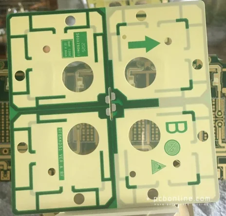
High-frequency PCBs are developed from antennas, but the antennas are not the loops you see anymore - two antennas are embedded in the circuit board as etched copper structures. So we can say that a high-frequency PCB is an antenna PCB that generates, evaluates, emits, and receives radio-frequency signals of more than 1GHz.
To better understand what a high-frequency PCB is, you should know its basic structure.
The basic structure of a high-frequency PCB:
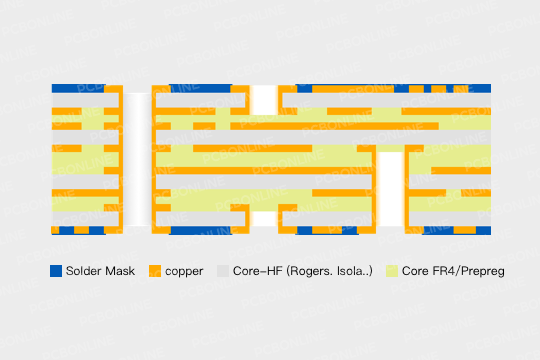
The most basic high-frequency PCB has 4 layers and consists of the RF system and the digital circuit.

- The upper layer or the front side of the high-frequency PCB is the RF system. It consists of a high-frequency circuit and two embedded PCB antennas.
- The second layer of the high-frequency PCB is the ground layer. It supplies power to the circuit and also shields the signal radiation and coupling.
- The third layer is the power layer, which supplies power to the circuit and also shields the signal radiation and coupling.
- The bottom layer or the backside of the PCB is the digital circuit.
Above is the most basic high-frequency PCB structure. Many high-frequency PCBs have 4 or 6 layers. To avoid signal radiation and coupling, high-frequency PCBs usually use many decoupling capacitors and high-frequency choke beads.
Part 2. How Does the High-Frequency PCB Work
High-frequency signals are transferred as electromagnetic waves. All PCB wires are supposed to transfer the signals rather than emit them. One PCB antenna emits them, and the other receives the reflected signals.
In the high-frequency PCB, the high-frequency circuit generates high-frequency signals, and the digital circuit evaluates the signals. Then the signals are transferred to one PCB antenna, and the antenna emits them. When the signals are reflected by the object, the other PCB antenna receives the signals. Then they are transferred to the high-frequency circuit for evaluation.
All the above functions of the high-frequency PCB are achieved thanks to the PCB's base materials. The high-frequency materials transmit high-frequency signals to antennas with the smallest possible attenuation.
In this way, a high-frequency PCB works like a radar application to spot objects.
Part 3. The Applications of High-Frequency PCBs
![]()
High-frequency PCBs work in the way of Radars, and in fact, a high-frequency PCB is the core component in a radar application. High-frequency PCBs have many applications in aerospace, defense, communication, automotive, and consumer electronics. These applications include:
- Radar scopes
- Transmitters
- Receivers
- Antennas
- Power amplifiers
- Low noise amplifiers
- Filters
- Mobile telecom products
- Automobile anti-collision system
- ...
Now you should know a high-frequency PCB's structure and functions. For more details on high-frequency PCBs, you should know their main types.
Part 4. Three Main Types of High-Frequency PCBs PCBONLINE Manufactures
There are three main types of high-frequency PCBs: RF 6-24GHz PCBs, RF 77GHz PCBs, and antenna-embedded PCBs. The classification is based on the distance from the object that the high-frequency PCBs locate.
- RF 6-24GHz PCBs: this type of high-frequency PCB transmits and receives 6 to 24GHz RF signals. RF 6-24GHz PCBs locate objects within 30 meters.
- RF 77GHz PCBs: this type of high-frequency PCB transmits and receives 77GHz RF signals. RF 77GHz PCBs can locate objects at a long distance. The signal wavelength that RF 77GHz PCBs generate is two-thirds shorter than RF 6-24GHz PCBs'.
- Antenna-embedded PCBs: this type of high-frequency PCB is developed from RF 77GHz PCBs. Compared with RF 77GHz PCBs, antenna-embedded PCBs have a small conductor width, conductor spacing, conductor tolerances, and rounded corners. The RF performance is improved, and the power consumption is reduced.
From the above, you can get a quite comprehensive overview of what a high-frequency PCB is. Another point you may want to know is:
The secret behind the expensive high-frequency PCBs is the base materials. These high-frequency base materials take up the most proportion of the circuit board's price. The base materials for high-frequency PCBs are PTFE, ceramic, FR4, PI, ceramic-filled PTFE, ceramic filled with hydrocarbon, etc.
- Low dielectric constant (DK). Small Dk means stable signals and little signal delay.
- Low dielectric loss (Df). Small Df means the PCB has a small signal loss.
- Low water absorption. Moisture elevates Dk and Df, so the materials should have low water absorption.
- Small thermal expansion and contraction coefficient and good thermal resistance. Otherwise, the RF performance will be affected seriously.
- Good chemical and impact resistance and peel strength. High-frequency PCBs are usually used in aggressive environments, so they should have these features.
The main high-frequency materials suppliers are Rogers, Taconic, Arlon, Taizhou Wangling, Ventec, and Nelco. And there are many high-frequency material series and models. You should choose the correct material model for your high-frequency PCBs. If you have difficulty in choosing materials, contact the experienced high-frequency PCB manufacturer PCBONLINE for free consultancy.
Part 5. One-Stop Solution for High-Frequency PCB Projects
Here is a one-stop solution provider for high-frequency PCB projects - PCBONLINE. From choosing materials, and antenna embedded design for manufacturing, and prototyping, to batch production and assembly, all can be done at one stop. PCBONLINE provides free one-on-one engineering support and DFX to high-frequency PCB projects.

Here are the technical strengths of the high-frequency PCB manufacturer PCBONLINE:
- Can manufacture the RF and digital interfaces on the same high-frequency circuit board.
- PCBONLINE's embedded antenna DFM technology minimizes high-frequency PCBs' conductor tolerance and corner roundness/roughness.
- Able to realize the embedded conductor structure design for high-frequency PCBs. And the antenna layer has low sensitivity.
- Our high-frequency PCBs have good impedance control and optimized RF performance.
- Realizes all types of vias for high-frequency PCBs, including blind vias, overlapping vias, staggered vias, skip vias, and buried vias.
- Stores ready-to-use high-frequency PCB materials in stock (storage within 45 days for quality assurance).
Online register and you will get $100 coupons for online purchases. And you can contact us online or by email.
Conclusion
This post tells you what a high-frequency PCB is and gives a complete yet easy-to-understand introduction to the high-frequency PCB structure, three types, how they work, and frequent applications. If you are developing a high-frequency PCB project for aerospace, defense, communication, automotive, or consumer electronics, PCBONLINE provides one-stop manufacturing solutions for you.


