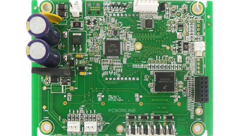
PCBA is a printed circuit board assembly. It is an electronic mainboard or module created by soldering components on a blank PCB.
A insists on insulating material sheets, copper foil, and solder masks. When it is soldered with desired components and passes inspections, it is a PCBA.
The following is what this article reveals details of PCBA:
Part 1: What is a PCBA?
PCBA or Printed Circuit Board Assembly is a term that refers to circuit boards surface mounted and/or through-hole mounted with electronic components, such as capacitors, resistors, and ICs. Some PCBAs can embed components, such as LTCC ceramic PCBs.
![]()
A PCBA includes a PCB and components. A PCB uses conductive traces and pads that are etched from copper layers, which are laminated between the non-conductive sheet layers. The components are soldered on the PCB to connect electrically and mechanically.
To ensure that the connection between the PCB and components works adequately, solder is welded or inserted into a blank circuit board and inspected to test its performance.
In a PCBA, copper traces in different layers are interconnected by copper-filled holes, and the electronic components are soldered on the PCB copper pads or inserted through the copper-plated through-holes. Besides, a PCBA can have two component-mounting sides.
![]()
A PCBA is a semi-electrical product for everything, from a small LED light to a large industrial control system. When PCBAs are installed with enclosures and other parts, they are box builds or final products. For example, the above image is a PCBA and its end product, a video projector.
Part 2: How do You Get a Custom PCBA
In this section, we will have a look at how to create a custom PCB assembly.
![]()
Step1. The first step in designing a custom PCB is to create a schematic view.
The required component is placed on a canvas and their pins are connected with lines that represent the electrical connections. The components usually are taken from a component library which is a part of the design software.
There may be multiple variations of the same components depending upon the type of package being used e.g. dual inline package or a surface-mounted chip. The packages may seem the same in the schematic view but are very different in the layout view where the board is designed.
Apart from the components and their electrical connections, power, and ground signals are also needed. Also, connectors have to be placed on the PCB to make a place for power and ground. The board is also required to be connected to external devices, such as potentiometers, LEDs, etc.
![]()
Step 2. Once everything is placed in its place, an electric rule check is run to ensure no evident faults.
These may include breaks in wires or connections or any missing connection to ground or power etc. Once the schematic is done, the board layout view is checked.
Step 3. The components are moved to proper places that make good sense.
Step 4. For the board production, signals are assigned to each layer and varying signals on a single layer cannot touch.
Step 5. After the signals are laid, a design rule check needs to run to ensure the proper placement of holes, traces, etc. These rules can be customized as well.
Step 6. If the design is approved, the design files can be uploaded.
The communication language of PCB fabrication is a Gerber file. Each board has multiple files, one for each layer. Another file known as the "drill file" is used to define where holes need to be drilled.
Step 7. Go to PCBONLINE's online quotation system and click "Browse Files" to upload Gerber.
When the Gerber is uploaded, it will run its error check procedure. It produces an image file of the PCB. You'll need to enter the PCB quantity you want.
![]()
Step 8. Check PCB specifications, choose the lead time, and click "Buy Now". Follow the next on-screen instructions. After that, it will take half an hour for PCBONLINE to audit your inquiry. Later, PCBONLINE will send an email to notify you about the order. You can send your bill of materials (BOM) and pick-and-place file to info@pcbonline.com for PCB assembly.
The one-stop PCBA manufacturer PCBONLINE ensures customer satisfaction and reliability. They build and assemble nearly perfect PCBAs with perfect working and neatness. The pricing also goes down with an increase in the number of PCBAs.
Throughout your PCBA project, one-on-one engineering support and considerate customer services from PCBONLINE are offered to you.
Here are some details of the PCBONLINE:
- PCBONLINE is a PCBA source-factory manufacturer with a group of in-house R & D teams of 100+ engineers and 500+ technicians.
- It manufactures 1 to 64-layer PCBs/PCBAs that are quite advanced, such as high-frequency PCBA, ceramic PCBA, rigid-flex PCBA, HDI PCBA, etc.
- It provides free services including the design for manufacturing (DFM), design for test (DFT), design for assembly (DFA), and design for excellence (DFX).
- It accepts custom PCBA orders for prototypes, small-batch, and massive production.
- It has a two-shift work system and the delivery is speedy (the fastest build time is 8 hours).
Part 3: PCBA Manufacturing - SMT and PTH
Nowadays, almost all PCBAs require surface mount technology, which is automatic. Through-hole technology (PTH) that is half-automatic is in less use.
SMT
![]()
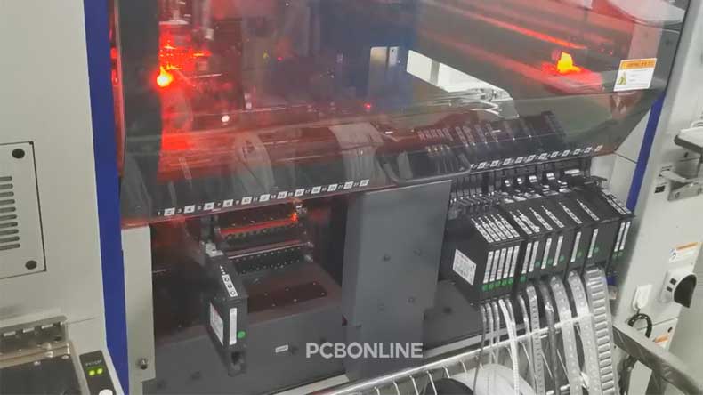
Surface Mount Technology or SMT stands for the whole technology of soldering components onto the PCB surface. In SMT, the components or SMDs have no or short leads only.
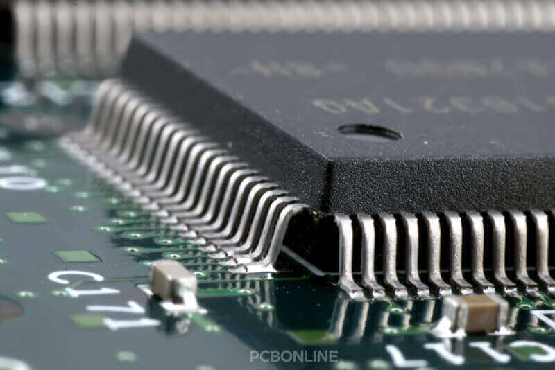
SMT assembly process is automatic and efficient. It includes solder paste printing on PCB pads, solder paste inspection, placing SMDs, reflow soldering, and automatic optical inspection (AOI).
SMT does not need the reservation of corresponding holes for the SMDs. And it is suitable for high-density circuits. At PCBONLINE, the smallest SMD footprint is 01005, and the finest pitch (center-to-center distance between adjacent SMDs) is 0.05mm.
PTH
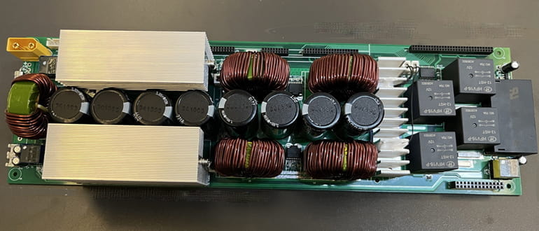
Through-hole PCB assembly, or PTH, means soldering component pins in through-holes on the PCB. THT is usually divided into single-ended, double-ended, and pin grid arrays.
Usually, the pins of the electronic components are inserted into the pre-set holes of the PCB manually. The PCBA is placed in a jig that exposes only the areas that need wave soldering and preheated. Then in the wave soldering oven, the THT component pins and the through holes are soldered.
If the PCBA requires different soldering specifications for different THT components, you will need selective soldering instead of wave soldering. From PCBONLINE, both wave soldering and selective soldering are available.
For massive PCBA manufacturing, SMT is more efficient and economical than THT.
Part 4: PCBA Inspections
Throughout the PCB assembly process, various inspections are required to ensure the robust connections and functions of the PCBA.
During PCB assembly, the PCBA inspections chronologically are:
- Solder paste inspection (SPI): After the PCBs are silkscreen printed with solder paste, they pass an SPI machine. Infrared cameras scan the solder paste, and the computer compares the specifications with pre-input standard specs to ensure that the size, thickness, and position of the solder paste are acceptable for soldering. Only after this inspection, can the PCB go to the placing surface-mount devices (SMD) step.
- X-ray inspection for BGA: If the SMDs include ball grid arrays (BGA), the PCBA should pass the X-ray inspection before reflow soldering. This inspection ensures that the solder balls of the BGA are intact and adequate for soldering.
- Visual inspection: Before reflow soldering, every effort should be made to make sure nothing goes wrong. So there's a quality control (QC) group on the SMT line to check the surface of the PCBA.
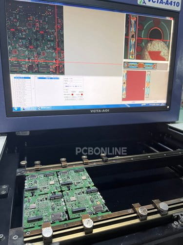
- Automatic optical inspection (AOI): After reflow soldering, the PCBAs should pass the AOI machine one by one, to guarantee no soldering mistakes, including solder bridges, component offsets, solder voids, tombstones, etc.
- One more visual inspection: After the AOI, the QC group needs to check the PCBAs to ensure no component and board aging due to too much reflow.
- First article inspection (FAI): In the PCBA prototype stage, 5 pieces are manufactured, and we randomly pick up one PCBA for the FAI. A specialized technician uses a probe pen connected to the FAI machine to touch the PCBA components one by one. The values of the PCBA components are recorded and compared with the pre-input ones. After the FAI, a report is generated automatically. We will send it to our client for review. Only with the client's approval, we can start massive PCB assembly.
- Another two visual inspections: Before and after wave soldering, our QC technicians visually check the PCBA to make sure nothing goes wrong.
- Multimeter inspection: In the PCB design stage, you will need to design pads for testing critical components on the PCBA using a multimeter. If you don't know how to do it or forget it, no worries, PCBONLINE will do it for you. After PCB assembly, we will use the two probes of a multimeter to touch the testing pads to ensure the critical components on the PCBA are workable. This is a necessary PCBA inspection.
- Functional testing: After PCB assembly, there is functional testing for PCBA, which is an optional inspection. The PCBA is put on a jig that powers on and connects with a computer. The computer will display the pass results of the PCBA on the screen.
- Thermal aging: Thermal aging is a PCBA inspection that checks whether the PCBA can work adequately after a long period of continuous work. The period lasts from 12 hours to 168 hours depending on the application requirements.
- Simulation test: After installing the enclosure, the PCBA is a box build or end product. To make sure the box build can work as expected, we can simulate the application field to see the working result of the product before the delivery.
THT assembly is not the end of PCBA manufacturing from PCBONLINE. You can have below PCBA inspections in the post-assembly stage.
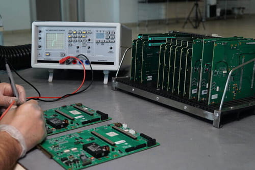
Besides, for flexible PCBs, the PCBA inspections include the tension test, bending test, hand sweat test, environment protection test, metallographic inspection, bridge test, withstand test, and impedance test.
Part 5. One-Stop PCBA Manufacturer - PCBONLINE
PCBONLINE provides one-stop PCB manufacturing and assembly. It focused on EMS PCBA services, including PCB fabrication, component sourcing, PCB assembly, and electronic value-added services including box-build assembly.
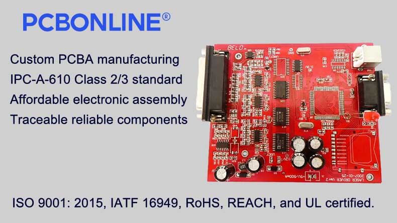
As a team of professionals building your PCBA, PCBONLINE ensures you make your work easy, efficient, and hassle-free.
PCBONLINE is a PCBA source factory manufacturer providing the most cost-effective electronic manufacturing services.
PCBONLINE provides custom PCBA on your meeting any of your requirements thanks to its strong capability.
PCBA manufacturing from PCBONLINE follows IPC-A-610 Class 2/3 standards and is medical and military-grade.
PCBONLINE offers design for assembly and one-on-one engineering support throughout the way.
For PCBA bulk production, PCBONLINE offers product R&D, PCBA samples, and functional testing for free.
Besides PCBA manufacturing, PCBONLINE provides IC programming, conformal coating, functional testing, thermal aging, and box-build assembly. If you have an interest in PCBA manufacturing, please contact info@pcbonline.com or chat with PCBONLINE from the online chat window on the right.
Part 6: Benefits of the PCBA
PCBA is a vital electronic semi-product of today's world. It offers several benefits, making it an important contribution to the modern world of electronics.
Time saver
It takes a lot of time for the traditional method of circuit connections to link the components. In contrast to traditional methods, the printed circuit board takes less time to construct a circuit.
Less cost with long-term reliability
In comparison with the traditional method, it would cost you less money and will be more convenient for use with maximum reliability for daily use.
Durability
The Printed Circuit Board Assembly does not have any wires that could be risky and tacky for the user. While the traditional method has copper wiring for the interconnection of different components of the PCBA. This makes it much more durable and reliable.
Great compactness
The PCB offers a simple platform to arrange the components compactly and efficiently. Due to this, a large number of components can be easily arranged on our platform.
Easy to get repaired
If any circuit component fails to respond, you can easily replace it with a new one. This makes the process of installation an easier and more convenient one.
Part 7: Applications of PCBAs
PCBAs are used in various industries due to their vital existence in the electronics world. PCBAs are crafted with a non-conductive material, on which copper sheets are spread widely. The use of PCBAs in electronic devices is very common today, and there are different kinds of PCBs. They may be single-sided, multilayer, or double-sided. They may be rigid, flexible, or rigid-flex.
Industrial Applications
![]()
PCBAs are necessary for industrial electronics. The Internet of Things (IoT) is the trend in all aspects, and PCBAs play a vital role. In smart transportation, cars on roads are monitored by industrial cameras, and PCBAs are critical elements in cameras. In all kinds of factories, pressure sensors, temperature sensors, and moisture sensors use PCBAs.
Medical Sector
As innovations develop, the healthcare industry is using rising numbers of PCBAs, unveiling new capabilities. In devices used for diagnostics, tracking, treatment, and more, PCBAs play a major role. In many instances, PCBAs must also follow strict sanitation requirements, especially those used for implants. Like the machines that compile and interpret these images, CT, CAT, and ultrasonic scanners use PCBAs. To obtain accurate heart rate readings, blood pressure, and blood glucose, PCBAs are also key elements.
Automotive
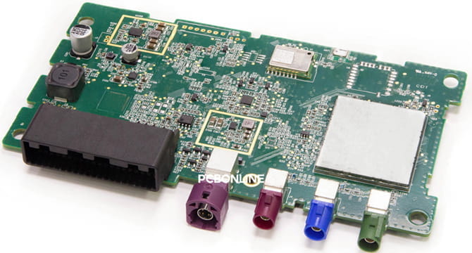
Several electronic components are being used by automobile manufacturers in their vehicles. PCBs were used mainly for items such as headlight switches and windshield wipers in the olden days, but now they operate many advanced features that make driving safer and easier for a lot of people. Before you install a PCBA in your car, you should check that the specific part of the car for which you are using the PCBA will be able to resist extreme temperature and vibrations.
Stereos and systems that incorporate navigation and entertainment do need PCBs. The engine management system and fuel regulators also rely on PCBAs.
Aerospace
There are similar specifications for electronics used in aircraft components to the ones used in the automotive industry, but aerospace PCBA may be subjected to even tougher conditions. In a range of aerospace devices, including aircraft, satellites, space shuttles, and radio communications systems, PCBA may be used.
To track the operation of the aircraft, pilots use different types of monitoring devices, including accelerometers and pressure sensors. Often, these displays use PCBA.
Military
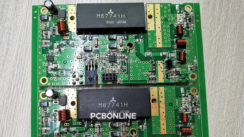
In defense applications, the military PCB assembly must be highly reliable and robust. PCBAs are required to operate radio communication systems and other essential communications. The control systems for different types of equipment, including radar jamming systems, and missile detection systems are based on PCBAs. Also, It allows indicators used by military members to track risks, execute military operations, and operate the equipment.
Consumer Electronics
PCBAs are helpful in smartphones, computers, and many other consumer goods that people use every day. PCBs with a large volume of connections are required to build small smartphones and laptops.
![]()
Wrapping Up
Suffice it to say that, PCBAs have a diverse range of benefits and applications that indicate their important use in everyday life. Additionally, PCBAs are cost-friendly, which in turn makes it easier to use them in different industries. PCBA with its application in different technologies can be used in different situations.
PCBONLINE provides one-stop PCBA manufacturing reliably, on time, and cost-effectively. If you need to design and build an efficient and durable PCBA for your system, PCBONLINE is your best choice.
Download


