
Managing heat dissipation is just as important as ensuring electrical performance when designing high-power or thermally sensitive electronic systems. In such designs, a thermal pad on the PCB is vital in maintaining component temperature, increasing reliability, and prolonging the product lifespan.
This article explains what a PCB thermal pad is, its structure, how it functions in thermal management, and how it's integrated into modern PCB designs with technologies like via-in-pad and copper-core multilayer PCBs.
What Is a Thermal Pad in PCB?
A thermal pad, also known as a thermal land or thermal slug pad, is a specially designed metal area, typically copper, placed on a PCB beneath components that generate significant heat.
It serves the primary function of transferring heat from the component into the PCB, where it can be dissipated into the surrounding environment.
PCB thermal pads are most commonly found under components with exposed thermal pads on their bottom surface, such as:
- Power ICs (e.g., regulators, PMICs)
- High-current MOSFETs
- LEDs
- Microcontrollers or FPGAs with high processing speeds
Note: While thermal pads are metallic and conduct heat, they are often electrically isolated from signal nets to ensure thermoelectric separation, which helps in maintaining signal integrity while controlling heat.
Structure and Materials of a Thermal Pad
A PCB thermal pad typically consists of the following features:
- Large copper pour: The pad itself is a thick copper area, typically part of an internal or bottom ground plane.
- Solderable surface: It is usually finished with surface treatments like ENIG, HASL, or OSP to ensure good solderability with the component’s exposed pad.
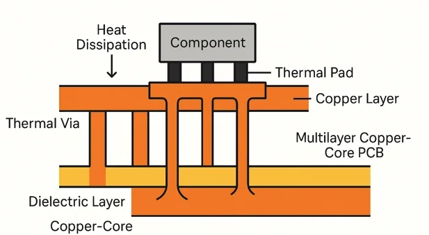
- Thermal vias (optional): Vias may be drilled through the pad to help channel heat to other PCB layers.
- Isolation or ground connection: Depending on design needs, it may be electrically connected to GND or isolated using non-conductive dielectric layers.
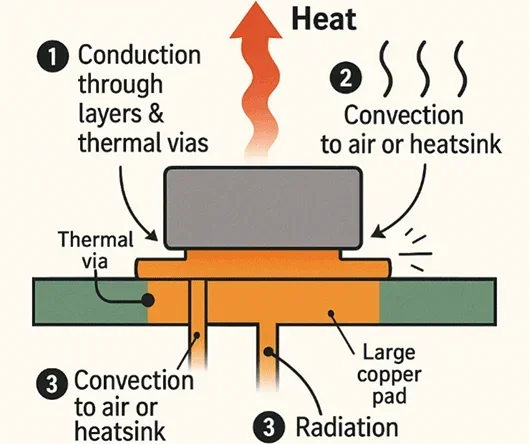
How Thermal Pads Dissipate Heat
Heat generated by a component is conducted from its thermal pad (on the package) down to the PCB’s thermal pad. From here, the heat is dissipated through three primary mechanisms:
1. Conduction through the copper layers and thermal vias to spread heat.
2. Convection to the air or heatsink attached to the board.
3. Radiation — minor but still part of the thermal equation.
Because the thermal conductivity of copper is high (~400 W/mK), having a large copper pad or connecting it to internal copper planes significantly increases heat dissipation efficiency.
Using Via-in-Pad for Better Thermal Management
To further enhance heat dissipation, thermal pads are often designed with via-in-pad technology, where thermal vias are drilled directly into the pad area.
Benefits of via-in-pad with thermal pads:
- Direct heat path from component to internal or bottom copper layers.
- Reduced thermal resistance.
- Minimized temperature rise in high-power components.
- Efficient use of PCB board space—ideal for compact designs.
As detailed in a previous blog on via-in-pad PCBs, via-in-pad is widely used in thermal management for high-power components. The vias are often filled and capped (via plugging) to avoid solder wicking and voids during reflow, ensuring strong thermal and mechanical contact.
Thermal Pads in Multilayer Copper-Core PCBs
For applications involving extreme power density, such as automotive electronics, RF power modules, and high-brightness LEDs, traditional FR4 substrates may not be sufficient.
Here, copper-core PCBs with thermal pads are used. These PCBs embed a thick copper or metal core layer to provide a dedicated heat dissipation path.
Key features of thermal pads in copper-core PCBs:
- Thermoelectric separation: Electrical and thermal layers are independently routed.
- High thermal conductivity: Copper cores efficiently spread and transfer heat away from components.
- Multilayer design: Allows integration of signal layers and power planes with dedicated thermal layers.
In copper-core PCBs, the thermal-electric separation design with thermal pads allows for advanced thermal management while supporting complex routing and component placement.
Design Considerations for Thermal Pads
When implementing thermal pads in your PCB design, consider the following:
|
Design Aspect
|
Best Practice
|
|
Thermal Pad Size
|
Match the exposed pad size of the component or slightly larger.
|
|
Copper Thickness
|
Use thicker copper (e.g., 2 oz or more) for better thermal conduction.
|
|
Thermal Vias
|
Use multiple small vias (0.3–0.5 mm) to create a thermal via array under the pad.
|
|
Via Filling
|
Fill and cap vias to prevent solder loss during reflow.
|
|
Solder Paste Coverage
|
Use paste masks with voids or dot patterns to reduce solder voiding.
|
|
Electrical Isolation
|
Use dielectric layers or clearance to isolate thermal pads if not connected to GND.
|
Applications That Rely on Thermal Pads
Thermal pads are essential for PCBs in the following applications:
- Power supply modules (DC-DC converters, motor drivers)
- LED lighting systems
- RF communication hardware
- High-speed processors and SoCs
- Automotive electronics (ECUs, battery management)
- Industrial power controllers
These designs operate at high current or switching frequencies, producing heat that, if not managed, can degrade performance and reliability.
Turnkey Advanced PCB Manufacturer Good at Thermal Pads
If you're planning a PCB that involves thermal-critical components, consider using via-in-pad structures or copper-core multilayer PCBs to achieve thermoelectric separation and reliable thermal management. How to bring your PCB into reality of high quality? You can work with a reliable turnkey PCB manufacturer, PCBONLINE, with R&D and EMS (electronic manufacturing service) capabilities.

Founded in 1999, PCBONLINE has two large advanced PCB manufacturing bases, one turnkey PCB assembly factory for PCB assembly and box-build assembly, stable material supply chains and strategic cooperation with electronic component manufacturers, and long-term cooperation with the top 3 mold and enclosure manufacturers in China for jigs/fixtures, molds, and enclosures.
Besides, PCBONLINE has an R&D team and professional CAM engineers for project development and DFM (design for manufacturing).
PCBONLINE can manufacture various types of PCBs with thermal pads and via-in-pads, such as FR4 PCBs and copper-core PCBs.
PCBONLINE is good at thermal management, including thermal path design, embedded and surface-mounted busbars, copper strips, thick-copper PCBs, ceramic PCBs, etc.
Provides one-on-one free and professional DFM (design for manufacturing) for PCB, PCBA, and box-build projects, including thermal-electric separation design for your project.
PCBONLINE manufactures, assembles, and tests PCBs with thermal pads to box-builds as a source factory manufacturer under one roof, from prototypes to massive production.
High-quality PCBA manufacturing certified with ISO 9001:2015, ISO 14001:2015, IATF 16949:2016, RoHS, REACH, UL, and IPC-A-610 Class 2/3.
When your project goes to the bulky production stage, PCBONLINE reduces the fees of prototyping, including its value-added services.
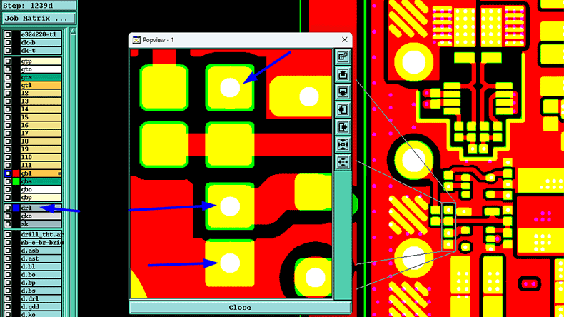
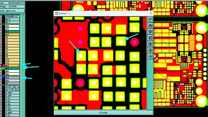
Examples of high-current PCBs with thermal pads
Below are high-current PCB projects with thermal management manufactured by PCBONLINE.
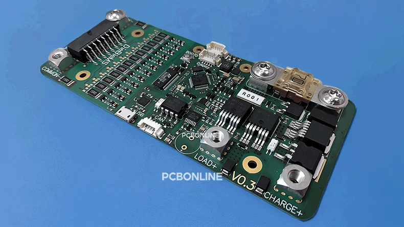
Example 1: battery management system supporting high currents and voltages
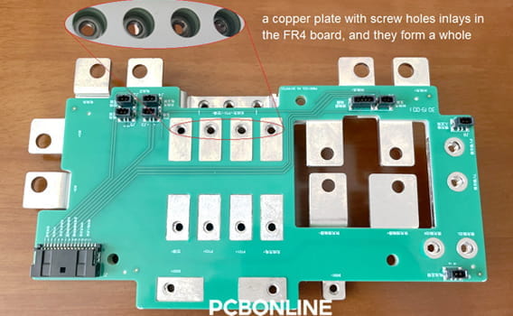
Example 2: adaptor board in EV high-power charging piles supporting large-current and high-power
By working with the one-stop PCBA manufacturer PCBONLINE, you can achieve better thermal stability, reduce component stress, and extend the life of your electronic products. No matter what application the PCB will be used for, such as automotive, industrial control, medical, military, aerospace, communication, agriculture, etc, you can work with PCBONLINE. To get a quote for your project to the turkey PCBA manufacturer PCBONLINE, contact info@pcbonline.com.
Conclusion
A thermal pad in PCB is a crucial feature that enables efficient heat dissipation from heat-sensitive or high-power components. It works by transferring heat through conduction into copper pours and planes, often enhanced with via-in-pad technology or integrated into copper-core PCBs for more advanced thermal control. To ensure the success of your PCB and PCBA project with professional DFM and high quality, work with the one-stop advanced PCB manufacturer PCBONLINE.
PCB fabrication at PCBONLINE.pdf


